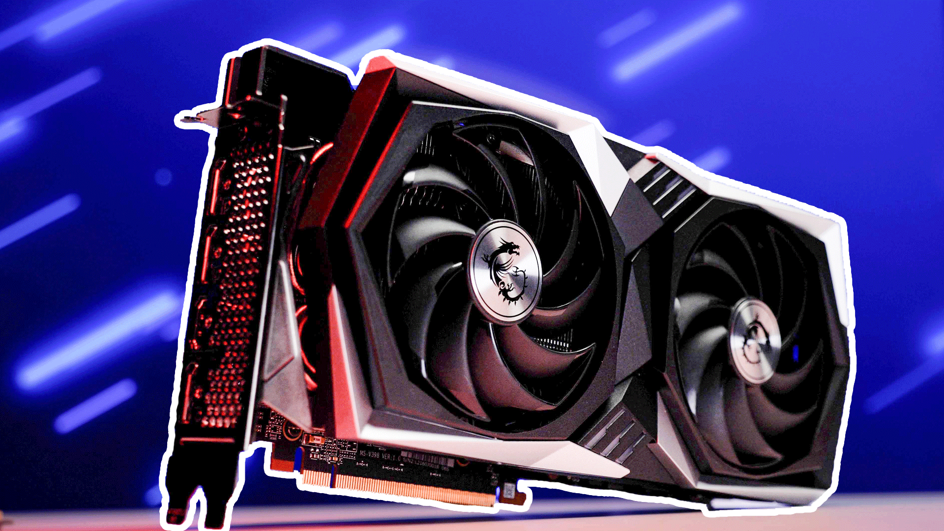
As previously mentioned, this card needs the extra cooling potential as it is marketed as both a low noise and high performance / factory overclocked Radeon RX 6700 XT. That is actually a tough combination to pull off… as the Radeon RX 6700XT are not known for being a cool running GPU at ‘stock’ frequencies.
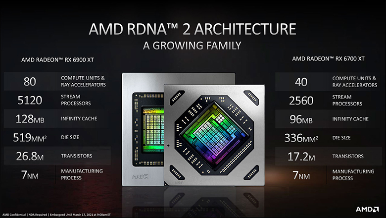
The reason the NAVI 22 XT is not easy to cool is twofold. First, and most obvious, is the fact that this core is designed to run in the 2.58GHz range. To put that speed in perspective, the last generation Radeon RX 5700 XT (aka NAVI 10 XT) was meant to only run at about 1900MHz. Yes, the NAVI 22 XT is bigger at 335mm squared vs. 251mm squared (and thus has much more surface area for cooling) but it has 17.2 Billion transistors (vs 10.3 Billion) running at higher frequencies. That is the second reason. 17.2 Billion highly clocked transistors all on the same 7nm TSMC node process. That is a lot of heat… even if officially the TDP has only been increase by 5 watts to 230 vs 225 of its predecessor.
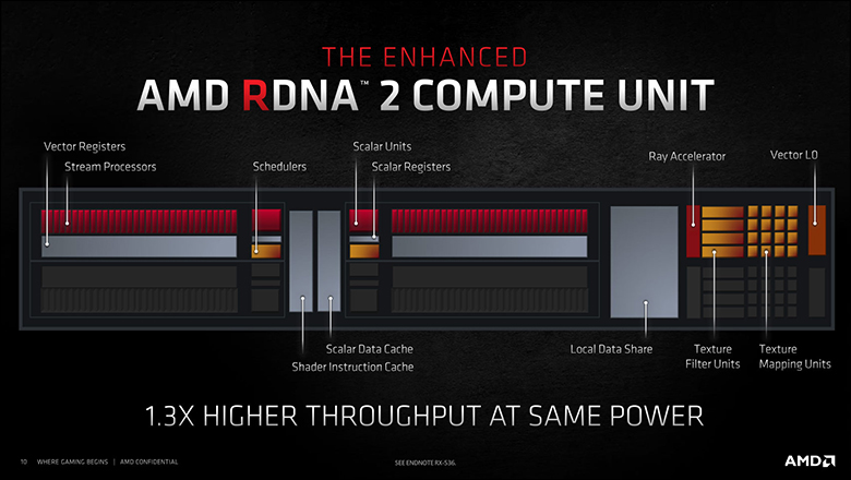
Thankfully, AMD has put all those transistors to good use and RDNA 2 is what the original RDNA core design should have been. While the ‘big picture’ has not changed and there still is 40 Compute Units (and all that goes along with each CU inside a Team Red core) in a “Dual Compute Units” (20+20) grouping on the silicon, each CU is now about 30 percent faster and consumes a lot less power. As such AMD was able to find room in the power package for 40 dedicated “Ray Accelerator” units (aka hardware based Ray Tracing).

Adding in hardware-based Ray Tracing however was not the only improvements that RDNA 2 / NAVI 2X brings to the table. For some, the most obvious improvement is Smart Access Memory (or SAM for short). S.A.M. is AMD’s marketing term for PCI Express’ Resizable BAR support that was actually added to the PCI Express standard back 2014 and integrated into the PCIe 3.0 standard. Yes, Resizable BAR is not a new idea. It is not even a newly implemented one (Windows 10 and Linux have had it for many years now). It just is a newly implemented one by video card manufactures… as it takes more than enabling just one component to make it work. Instead, the motherboard, the OS, the video card, and drivers/firmware must all work in harmony to let the CPU directly access more of the GPU’s memory. Furthermore, the end-user also has to manually enable “above 4G decode” or “>4GB MMIO” in the BIOS… and this last caveat is a big reason why video card drivers have left it at its (in Windows at least) default of 256MB and called it ‘good enough’.
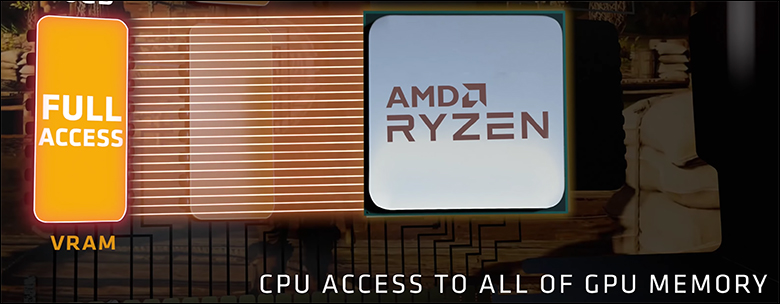
The upside is when you do let the CPU have direct access to more of the memory the efficiency of CPU to GPU communications is increased by a notable percentage. It however, regardless of what any speeches or marketing material may have inferred, cannot and does not widen the memory path between the two. It also does not increase the speed of the PCIe bus. All it does is allow the CPU and GPU to talk more efficiently with each other. That however is nothing to sneeze at. A couple percentage points in lowered latency can pay out noticeable dividends in Frames Per Second.
There are however a few downsides beyond all the moving parts involved. Firstly, when talking about MS Windows… R-BAR’s are tricky to get to work. The more possible combinations of video cards, motherboard chipsets, and CPUs there are… the more headaches the video card driver team has to deal with. This is why AMD has limited it to AMD Ryzen 5000 and 3000 series CPUs running on AMD 500 series chipset based motherboards… and only for RX 6000 series GPUs (obviously future variants of the above will also be supported). No Intel CPUs. No older RX 5000 GPUS, and certainly no NVIDIA GPUs.
Needless to say, phrases like ‘monopolistic behavior’ and “senate inquires” and “EU fines large enough to pay for more EU bread and circuses” do spring to mind. Thankfully for consumers, and AMD investors, NVIDIA has already nullified SAM via their own implementation of this PCIE-SIG standardized feature. Arguably NVIDIA has one upped AMD as any RTX 3060Ti or higher card running on Intel 10th (or newer) running on 400 series (or newer) motherboards, or AMD Zen 3 running on 500 or even 400 chipsets can also get Resizable BAR support via March 30th 2021 (or newer) drivers.
This nullification and one upmanship is why the other improvement is actually more important… as NVIDIA can not just go ‘here hold my beer’. This low-level improvement is Infinity Cache. An idea taken directly from AMD’s EPYC Processor design team (and is a great example of the ‘synergy’ we have all been waiting for since AMD purchased ATI many years ago). At its most basic this Infinity Cache can be considered a last-level / L3 cache buffer that resides in the middle of any and all Compute Unit clusters For frame of reference think of the location of the I/O controller ‘chiplet’ surrounded by the Zen chiplets in a modern AMD processor… just at the silicon level not chiplet level.
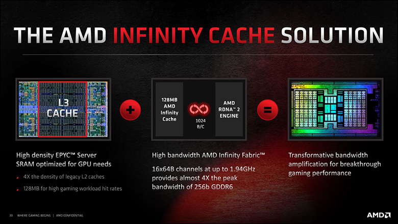
As the name suggests this cache can be access by any Compute Unit via the Infinity Fabric and thus allows for much lower latency compared to the GDDR6 memory buffer. The only downside is on RX 6900 XT and RX 6800 XT it is ‘only’ 128MB and on NAVI 22 XT it is only 96MB. To be blunt, these smaller NAVI 2x GPUs could really have used 128MB or more of Infinity Cache… as they are running on a 192-bit memory bus. Not 256-bit like the bigger variants of NAVI 2x. This smaller memory bus does put it at a distinct disadvantage compared to its direct competition… both of which use a 256-bit wide memory bus.
On the positive side, AMD did have the choice of either using 6GB or 12GB of onboard RAM and specified 12GB of fast GDDR6. While GDDR6 may not be as fast as GDDR6X (let alone HBM2 or HBM2E) it is a lot more reasonably priced. This is considered a more mainstream / entry-level option so we have no real issues with the use of Samsung GDDR6 memory. Especially when said Samsung (K4ZAF325BM-HC16) memory clocks in at 16GHz (effective) and not 14GHz (effective). That is both 4GB more and 2GHz (effective) faster than what NVIDIA’s GeForce RTX 3060Ti/3070 cards come with (typically Samsung K4Z80325BC-HC14).
Make no mistake. This card may indeed come with 12GB of rather fast GDDR6 VRAM onboard. It may also indeed come with a factory overclock and excellent custom cooling solution. Neither of these things are miracle workers. So if the large “1440 QHD” on the front of the box did not make it clear, the RX 6700 XT is not really going to excel at 4K resolutions. Having 32 less CU’s of the RX 6800 XT (40 vs 72) may not mean only 55 percent of the performance (especially when comparing AMD stock RX 6800 XT’s to this beast from the east)… but the 4K resolution abilities may be a little on the anemic side. Put simply 12GB of good VRAM simply means that memory capacity is not going to be a bottleneck. The ‘real’ bottleneck at higher resolutions is the 192-bit wide bus. Even NVIDIA and their 3060 TI have moved away from 192-bit and gone for 256-bit buses. This narrow(ish) bus is the Achile’s heel of all RX 6700 XT’s. As such there was/is nothing MSI could do about it. It is what it is.
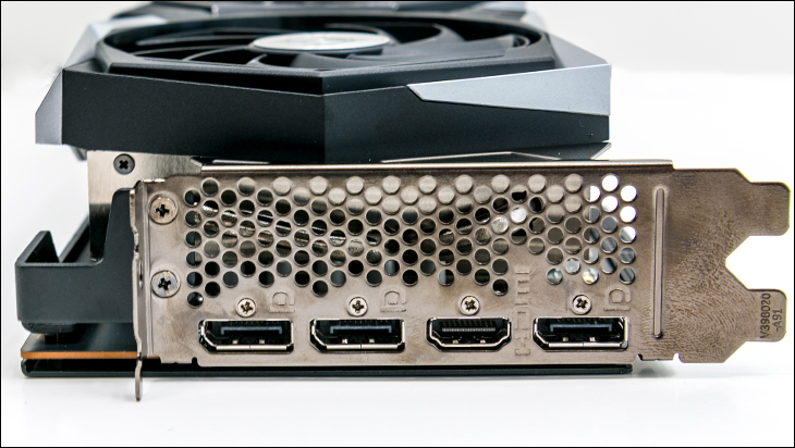
When it comes to connectivity options MSI has opted for the bog-standard configuration. That means three full sized DisplayPort’s which are all DP1.4a compliant, and a single HDMI which is 2.1 compliant. This actually is a bit of a disappointment as this is a three-slot card and yet two slots worth of space are not used. Instead, all four ports are in a row on the slot nearest the PCB.
