The reason that Intel has been able to outperform AMD’s processors can be summed up in one simple acronym: IPC. IPC or Instructions Per Clock is a simple, yet effective, method of judging how efficient a CPU design is as it does not matter how fast the core is clocked, it does not matter how many cores there are… as the IPC of a design will remain the same. Oh sure the overall performance will go up when comparing a 3Ghz to a 4Ghz version of the same design, but the actual number of instructions per clock cycle it can handle will be the same.
This is the area that AMD has fallen a bit behind in when compared to Intel. This is not because of a lack of talent and simply a lack of resources. This should come as no surprise as Intel literally has a yearly research and development budget in the ten-figure range. When you ‘you’ as a company can literally throw hundreds and hundreds of millions and dollars at CPU architecture design every year ‘you’ can release a new architecture a lot faster than a company with a lot less resources. This is why even though AMD’s Excavator team have refined the underlying design and reached performance levels they could have only imagined of when its ancestor Bulldozer was created Intel has been able to outpace them.
AMD really is the scrappy underdog of the computer world and their ‘make do with less’ attitude is why they are the only x86 CPU manufacture to still be standing and not be crushed into dust by the Intel juggernaut. So AMD knew they had a problem, they knew they were falling further and further behind – to the point where simply pushing the speed of the core would not let them stay competitive – and they decided to do something about it.
This is how Zen came about… and the dream of Zen was rather ambitious – to create a new design that had a 40% higher IPC than Excavator. To put this goal in to perspective they basically wanted to create a design that when running at a mere 2.8Ghz could perform the same as a 4Ghz Excavator core. Let the shear audacity sink in… and then realize that Intel is perfectly happy, and consider it a good return on their investment, when their new architecture is 5-10% better than their old one.
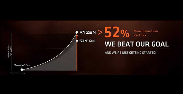
So did AMD succeed at their intended goal? Well yes and no. You see Zen is indeed did hit 40% improvement… but no AMD’s team did not stop there. Instead they created a monster that is 52% better. Yes, and with all other things being equal (which they are not… more on this later), a single 1.92Ghz Zen core will basically perform the same as a 4Ghz Excavator core. Basically, Zen is an AMD ‘Athlon 64 X2’ sized leap forward for them.
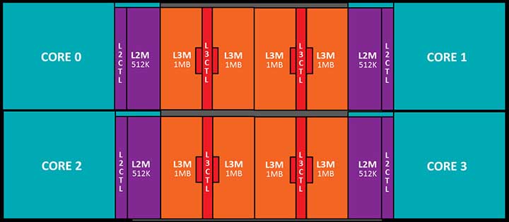
So how did AMD go about creating this miracle? They rethought about how they were designing CPU’s in the past and took a page from their APU and GPU design teams. At Zen’s heart beats a modular building block called a CCX or Cpu CompleX. Much like a AMD’s “Compute Unit” APU building block this CCX block is made up of a bunch of prefab parts. Want a bigger CPU… add more CCXs. Want a smaller one… turn off parts of a CCX. To be a bit more precise each ZEN CCX block houses four cores, 64K of L1 cache per core (256KB total), 512KB L2 cache per core (2MB total), and 8 MB of L3 cache that is shared across all four cores.
Unlike previous cores a Zen CCX has native simultaneous multi-threading (SMT) technology baked right in allowing each core to process two threads at a time… just like Intel cores… ish… as AMD’s SMT is arguably smarter/better/more efficient than Intel’s ‘hyperthreading’ design (right now). Put another way each four core CCX block can handle eight threads simultaneously. Yes no more ‘core and a half’ math needed when thinking about AMD processors as each core really is a full blown core that can handle all duties. Thus an 8 core Zen based Ryzen CPU is indeed an 8 core processor and not a 6 core with 2 more half cores for specialized work only.
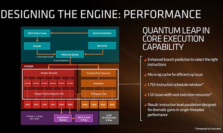
Drilling down further each core in the CCX can not only handle two threads at once but AMD has given the Zen design a much-needed performance boost thanks to a much quicker instruction scheduler. To think of what an instruction scheduler is and does, imagine the I.S. is the foreman on a worksite directing what tasks go to what parts of the ‘job site’ and who will work on what (i.e. parts of the core). Basically, this foreman is a heck of a lot faster and smarter than its predecessor and a big reason why the IPC is 52% higher.
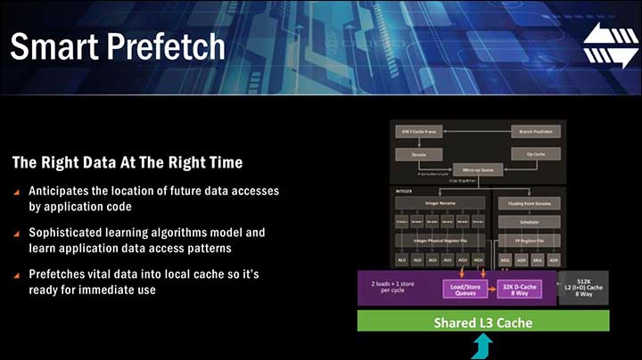
Backstopping this desperately needed scheduler is some really… really advanced predictive math for the cache buffer. You see a modern CPU vastly outstrips even the fastest external memory going so in order to keep the CPU actually working on tasks and not waiting for the equivalent of a cement mixer to come from across town, the CPU itself has to ‘pre-order’ data to fill its ‘on-site’ buffer (i.e. it’s extremely fast L cache buffers). This is called ‘pre-fetch’ and if the pre-fetcher gets it wrong the CPU cycles that were used on going down that rabbit hole are wasted and the buffer may even need to be flushed before the CPU can do the actual work that comes in next. Basically, when it works the CPU hums along at max capacity and the overall system performance is outstanding… but when it gets it wrong often the system gets ‘slow’.
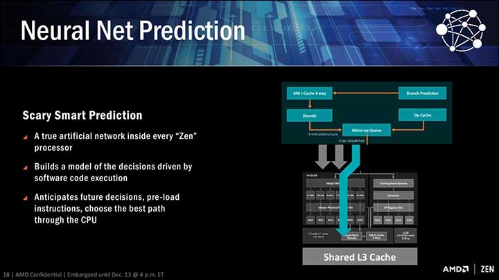
AMD’s improvement in this predictive analysis is called Neural Net Predication and is based on some pretty advanced deep learning and machine intelligence science. No its no SkyNet, or even StarTrek’s Data… but it is a lot better than its ancestors. How it stacks up against Intel and their mega-budget remains to be seen… but AMD states the CPU ‘learns’ your habits and adjusts its pre-fetch routines based on your usage pattern… which is a little creepy… as do you really want the CPU knowing your web viewing habits… and judging you based on them?! In all seriousness it doesn’t judge it just does what is best for your habits… no matter how odd they may be.
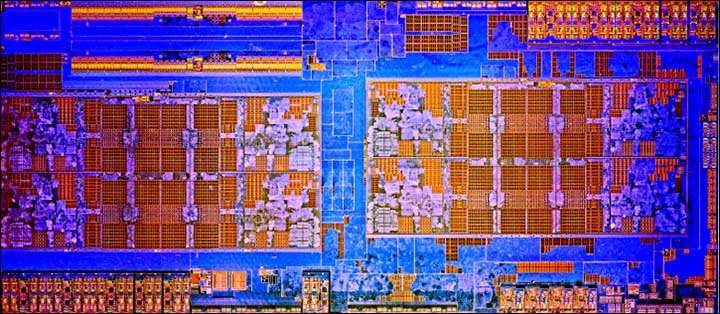
Zooming out a bit, a Zen CPU (or the eventual Zen APU’s for that matter) does not need to rely upon just one CCX building block… or even a full building block. For example a Ryzen R7 CPU makes use of two full CCX’s, but smaller ones (like the APU ‘G’ series) only need one or one and a half. When more than one is used these CCX’s are connected via what AMD calls Infinity Fabric… but can be considered AMD’s next generation processor interconnect that sits on top of the CCX’s and allows them to communicate with each other. In other words, you can consider it a modified/improved/etc version of AMD APU’s Heterogeneous System Architecture (HSA) idea. This additional layer is however why you can expect Ryzen ‘G’ processors with built in GPUs to land in the future… and carry on the AMD APU tradition.
Now as this CCX is modular all the way down to the core level AMD can easily disable 1, 2 or even 3 cores in a CCX to create smaller core-count Zen processors. For example, disable one in each CCX and you have a ‘6 core Zen’ (higher Ryzen R5 models). Disable two in each CCX and you have a ‘4-core Zen’ CPU (AKA Ryzen 3 and lower Ryzen 5). This not only allows AMD a lot of flexibility in creating tailor made Zen processors for a wider range of the marketplace, it allows them to use Zen Ryzen cores that don’t quiet pass muster at the full CCX level in the lower Ryzen series – more on this later in the review.
So in summary Zen is a lot faster at single tasks, is a heck of a lot smarter, is much more modular and overall a radical improvement for a single generation. This is exactly what AMD needed and we are glad to see that is what they did.
