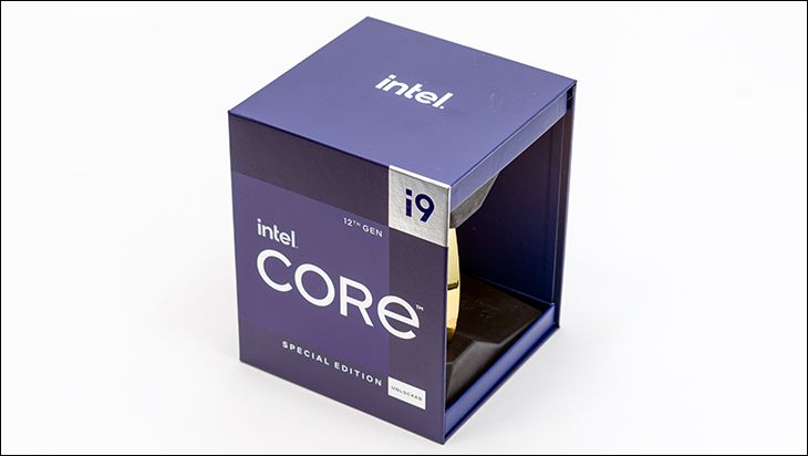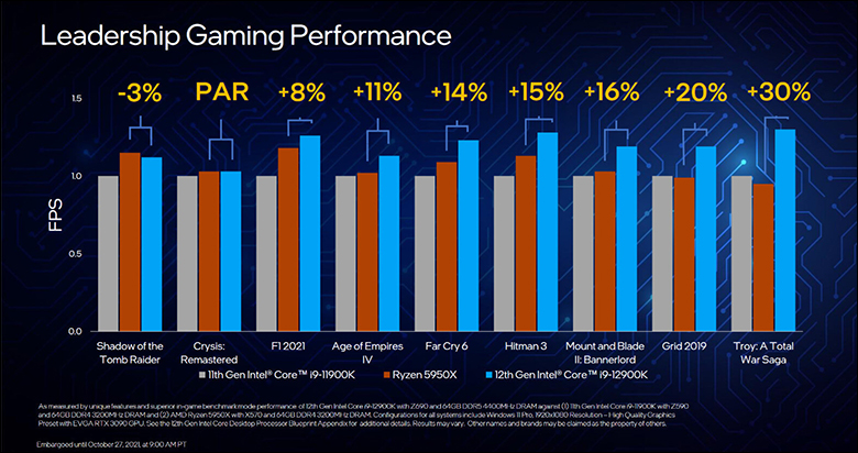
Intel has made a big deal about IPC and wanting to regain the crown AMD and their Zen 3 snatched from them recently. Intel claim that Alder Lake offers 19 percent IPC improvements over their 11th gen… and after testing they are correct. With an asterisk and an ish. The asterisk being that there is only 8 p-cores that are blazing fast in this ’16 core’ i9. IPC is all well and fine as long as you understand that only 6-8 threads are going to be blazingly fast because of it.
The ‘ish’ comes into play in that the new Gracemont cores may be incredibly fast for ATOM cores… but performance does drop off as more and more in a given block are loaded. Basically, when only 1 of a 4 e-core block are active they have plenty of cache and thermal headroom to handle the task. Handle it so well you would almost think they were a couple generation old Intel CPU core(s) and not freakin’ Atom cores. However, when all four are active performance does suffer. There is still not enough cache to keep it from having to go out to L3. Also, Intel is being rather aggressive in keeping their Processor Base Power (and thus power consumption) as low as possible. Overclocking can indeed help… but they do get toasty rather fast once pushed above their stock Turbo settings.
Since the e-cores are optimized to sip as little power as possible (a little more than half of a Skylake core) and taking up as little room as possible (a 4 e-core block is about the size of one 1 p-core), while also providing a lot of power (claims put it at about 8 percent higher performance clock for clock than Skylake) they are not HyperThread enabled. That is why the Core i9-12900K and Core i9-12900KS are classified as a 16 core, 24 thread CPU.
The end result of that combination of e-core issues is that if one is active you can almost consider it the same as a similarly clocked 7th or 8th gen Intel core, but all are active? Then its ATOM roots start showing and showing badly. Of course, this only holds true when either all e-cores are on high demand threads, or you are using a ‘core aware’ application that can crush 16…32… even 64 core processors. When dealing with 3 or sometimes even 2 low demand threads and only 1 (or sometimes 2) high demand on a 4 e-core block… that e-core block is rather peppy and you will probably not know for sure if a thread is on an e-core or a p-core. That is rather impressive, but still something to consider when comparing Intel to AMD for your next upgrade.
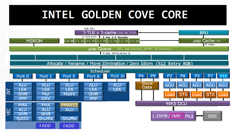
Moving on to the star of the show. The ‘Golden Cove’ microarchitecture is also rather advanced and has a lot of buffed features versus the backported Cypress Cove design it replaces. While AMD was saying that going beyond a 4-wide instruction decode strategy would result in potentially worse performance… Intel went ahead and did a 6-way. Then doubled the fetch bandwidth to 32bytes per cycle to help feed that hungry beast. Though to be fair, Intel is well, well aware of AMD’s point. That point being that if the decoder gets it wrong… it is a massive (double digit) penalty in lost processor cycles.
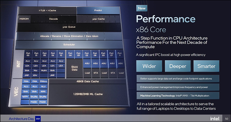
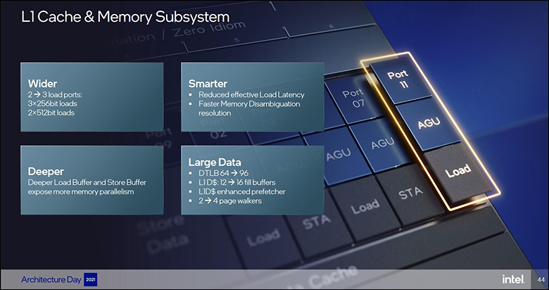
To help ensure that this does not happen all that often, Intel has done their best to make sure that the core did not have to rely on a costly decode operation at all. To this end they also went ahead and nearly doubled the micro-operation (‘μop’) cache from an already large 2,250 entries in the 11th gen to 4,000 entries. Then basically increased its bandwidth from 6 to 8. Then doubled the L1 instruction cache entries from 128 to 256. Then increased the L1 data fill buffers from 12 to 16.
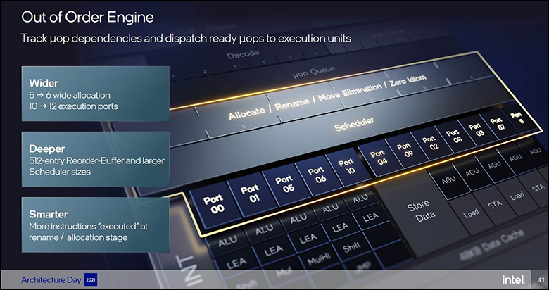
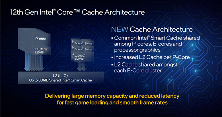
Since someone was already holding their beer… they even increased the L2 Branch target buffer from an already large 5,000 entries to a whopping 12,000 entries. Improved the pre-fetchers via a “full-line-write predictive bandwidth optimization” strategy (aka fuzzy math that makes even most genius head hurt when they try and think about it). Then to just add salt to the wound they increased the re-order buffer from 352 to 512 entries to improve out-of-order instruction performance. About the only thing that is not massively improved is the execution width of 12 (up from 10)… which is lower than the e-core’s 17. The same is somewhat true of the L3 cache. On the one hand the i9 now has 30MB (up from 20MB) and the i5 has 20MB (up from 12MB)… but it is spread out over more ‘cores’. Basically, instead of 2MB per core it is now 1.875MB for the i9 and 1.66MB for the i5 (ironically enough the i7 and its 25MB of L3 cache is actually more per core at 2.1MB).
Needless to say, that is a lot of low-level improvements. A lot of low-level improvements that take a lot of time and effort to get right. When they do get it right, as they obviously did here based on test results… it all but guarantees higher IPC in the real-world. Intel states it is an average of 19 percent improvement over last gen, and in many cases they are actually being rather conservative. Of course, in other cases they are being… overly optimistic.
To be fair, IPC has not been Intel’s sole focus as performance per watt was just as important. They also wanted to improve multi-threaded performance… as the software world is slowly becoming more and more multi-threaded. Splitting their focus means less improvements in any on area but better overall improvements. The most obvious multi-thread improvement is the Memory-level parallelism (MLP) capabilities. Here they have been improved with Golden Cove being able to handle 48 outstanding requests from 32 in the 11th generation. Once again, something that takes a lot of time and effort to implement… but when implemented properly boosts overall multi-thread performance higher than ever before.
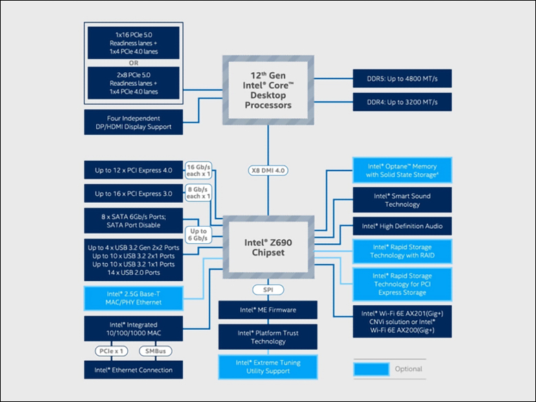
The other big improvement is both highly exciting and yet highly frustrating at the same time. We are of course referring to PCIe 5.0… of which there is a grand total of zero PC components available right now. Maybe mid to late next year we will see GPUs and maybe even NVMe drives (if Phison is to be believed) take advantage of this massive bus, but it is a ‘future proofing’ type feature. Also, Intel has not increased the number of lanes powered by the CPU. It still is 20. In fact… its 16 PCIe 5.0 + 4 PCIe 4.0 lanes… with the four lanes meant to be used by the motherboard manufacture for a M.2 drive. In other words, if PCIe 5.0 NVMe drives start appearing not every motherboard’s M.2 slot will be able to run them. In many instances owners will have to purchase M.2 to PCIe board adapters and split their 16 PCIe 5.0 ‘GPU’ lanes into two x8s – thus nullifying PCIe 5.0 x16’s bandwidth advantage over PCIe 4.0 x16.
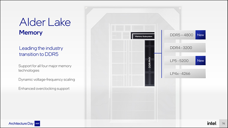
On the positive side, in order to handle DDR5 and PCIe 5.0 bandwidth requirements Intel has beefed up the internal interconnect bus(es). The Compute Fabric (what allows all the blocks of e and p cores to communicate with each other and their cache) is a whopping 1000GB/s (or one frickin’ TeraByte of data per second). The Memory fabric portion of the internal interconnect is now rated for 204GB/s… or basically the same as what Intel uses in their 8-channel Ice Lake servers CPUs. Also beefed up is the CPU to chipset bus which is now 64GB/s… aka PCIe 5.0 x16. That is a lot of uber wide buses that should help the spice… err… data flow… and flow it must.
Taken as a whole and the 12th Generation Core I-series is the most advanced and most radical departure since the inception of the Core I-series landed.
