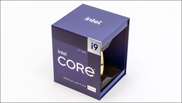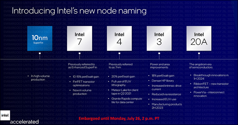
As is our typical Modus Operandi let us start with the most obvious changes between Rocket Lake (11th gen) and Alder Lake (12thgen). Alder Lake is built using Intel’s “7” fab process. This is both excellent news, and yet a wee bit disappointing. It is disappointing as a “7” in modern Intel speak does not mean 7nm. It means a 10nm “Enhanced SuperFin” node process is used. The seven comes about as it is about the same size as what TSMC claims as a 7nm node size. For simplicity, and a delicious dose of irony, think of AMD having to label their early X2’s “4800” or “4400” so as to compare more ‘fairly’ to Intel’s single core CPU offerings. This time it is Intel behind the eight-ball needing to clear the air and right some misleading ideas floating around in the modern consumer’s zeitgeist.
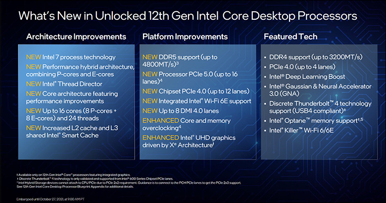
It is good as it puts a pin in on all that craziness over ‘14nm+++++++’ that garnered way too many page clicks for trolls. It is also good as this means a noticeable increase in performance and decrease in power consumption (smaller transistors switch faster and use less power doing so). For example, when Intel pushed out a trickle of 10nm Tiger Lake mobile CPUs earlier this year, they put it at about a 10-15% increase in performance per watt just from going from their latest 14nm node process to the smaller 10nm node fab size. That kind of improvement is nothing to sneeze at.
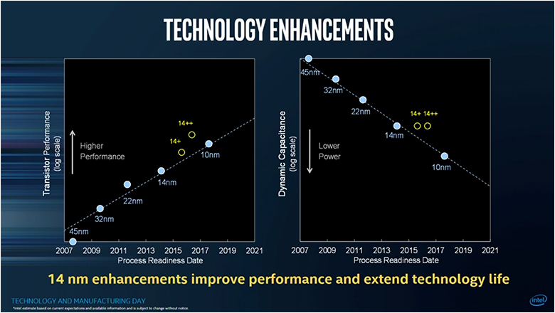
It is also good as this is not the original 10nm fab process. A process that Mark Bohr back in 2017 poo-poo’ed as being inferior to the 14nm++ node process (https://vimeo.com/intelpr/review/210691247/77b64a2bcd)… and is a big reason Crimson Canyon NUC’s underperformed as badly as they did. It is also not the “10nm+” that made it to market(ish) via Tiger Lake BGA CPUs. Instead, Alder Lake usess a third generation 10nm fab process. An enhanced process which promises another 10-15% gain over the second gen / ‘10nm SuperFin’ node process.
Using a smaller node process is also good as it allows Intel to fit more transistors into each square millimeter of silicon. Think 100’ish MTr/mm² (mega-transistor per squared millimeter) vs 37.5 MTr/mm². This combination, in conjunction with a slightly large socket size (more on this in a moment), is how Intel can fit more cores inside their 12th Generation Core-I series vs. the previous generations of CPUs.
It however does not mean one should expect an average 20 percent or better performance improvement. Instead, this freeing up of power has been used for more… well… everything. More cores. More onboard L3 cache. Better IMC. Basically more. Of everything. Without an increase in overall max power consumption.
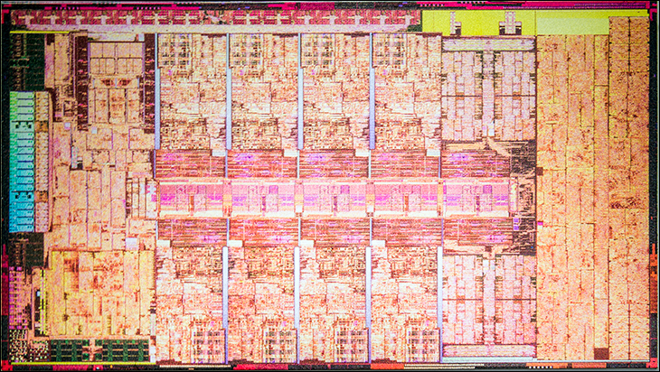
Before we go over that however, there is one thing we have to make clear: There Is No Such Thing As A Free Lunch. When you put more transistors into the same amount of space and feed them the same total amount of power as before(ish)… heat is an issue. Intel is well aware of this and have taken multiple steps to curb heat production and handle said heat when it is created.
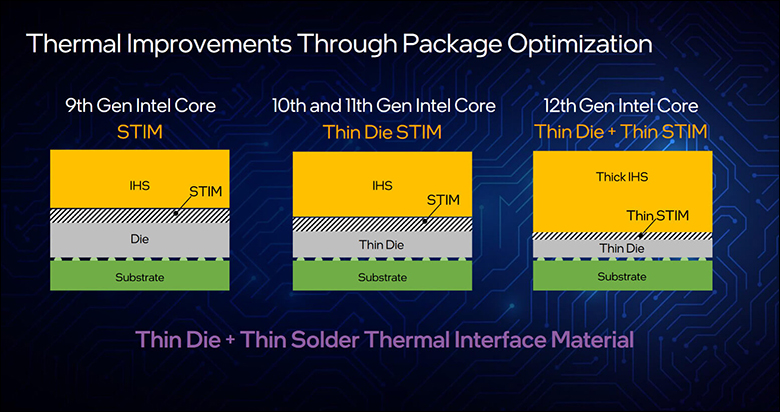
The first step is physical. Modern CPUs are flip chips with the ‘bottom’ silicon substrate layer being ‘on top’ and the transistors below them. A lower z-height in this substrate (aka thinner substrate) means that the heat from the cores has less heat insulating bulk to travel through before it reaches the IHS. In the 10th they started shaving some of this substrate and making the copper IHS (and used solder TIM) thicker, then they thinned it again for the 11th gen… and now its even thinner. Think under 0.5mm tall. Then to further improve heat transfer to the IHS, Intel also made the Solder Thermal Interface Material (aka STIM or sTIM) thinner. Interestingly enough, Intel did not specify a lower Z-height for their new socket 1700 specification. Instead, they kept it the same as Socket 1200. This means more copper in the IHS which in turn means the Integrated Heat Spreader is even better at its job than its predecessors.
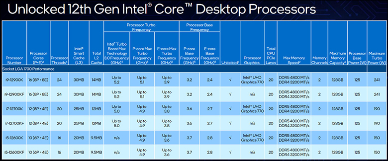
Of course, it must be better than previous IHS as the ‘hot spots’ are not smack dab in the middle of the socket. They are offset either slightly above or slightly below the center line (depending on which cores are active and what s1700 CPU you are using). When pushing their Maximum Turbo Power limits they can get toasty… and when manually overclocking them even further they get down right hot. Needless to say, you are going to want a good cooing solution (preferably water based) capable of handling over 250 watts of heat if using the Core i9 and over 150 if the Core i5. Though to be fair that is a downgrade for the Core i5 (the last gen was a fireball that also needed a cooler capable of handling 250+ watts of heat), and pretty much par for the course for the i9 when compared to the 10th or 11th gen Core-i9s.
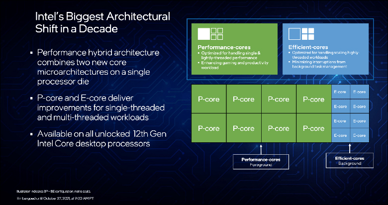
The next way Intel is combating heat is simple: make less of it whenever possible. By taking a page from ARM processor designs Intel’ latest mainstream CPUs no longer consist of all the same core types. Instead, they are broken down into two separate and distinct types: efficient ‘e-core’ cores, and performance oriented ‘p-cores’ cores. The P-cores are basically what was supposed to be the ‘tock’ to the 11th generations 10nm design, and the e-cores are actually next gen ‘Atom’ cores.
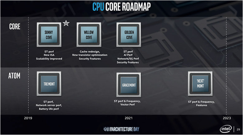
Of the two core types in this hybrid architecture the “Gracemont” Atom cores are the most intriguing. This is not because of rumors of Intel using ‘ARM’ cores… as they are not ARM based cores. They are x64 cores. Instead, their inclusion is intriguing for the simple fact that the Atom CPU design philosophy is one of efficiency above all else… including computational power. That is a radically different philosophy than previous gen desktop CPUs. Basically, Atom CPUs are meant for ultra-low to low powered devices such as Network Attached Storage devices, routers, portable devices, and ‘System On a Chip” type devices where TDP (or “Processor Base Power” in latest Intel speak) requirements are for 10(ish) watts or less. Devices which typically run ARM SoC’s that Intel want manufacturers to convert over to Intel SoCs. Put bluntly Atom design is the antithesis of what desktop CPU’s are all about.
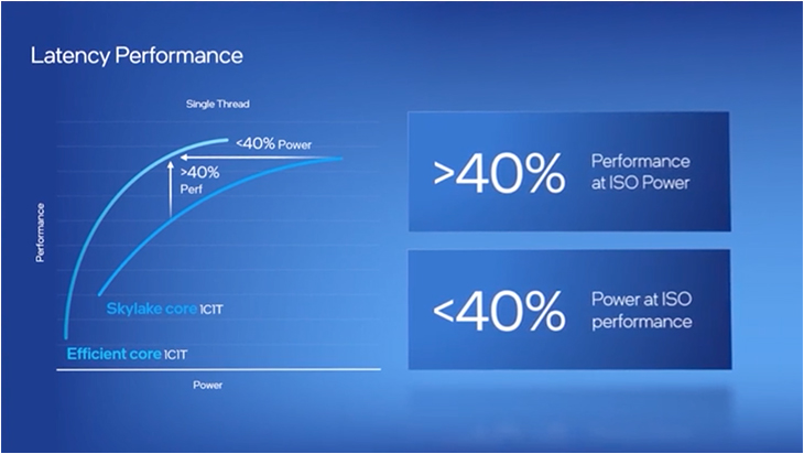
To be fair, these are not typical Atom cores. They replace the ‘Tremont’ design used in Intel’s actual first hybrid CPU design / trial run – ‘Lakefield’. As such they don’t have a 10watt Processor Base Power limit like those found in inside upcoming Android tablets or phones or etc. etc. Instead, their Processor Base Power is part and parcel of the entire Alder Lake Die package. Therefore, even though they may have a base frequency of 2.4GHz (12900k) or even 2.8GHz (12600K) those numbers don’t really mean anything. Sure, they will idle along at that (or lower) if they do not need more power to complete the task they have been assigned… but they can (and will) boost up to 3.2GHz (12900K) or even 3.7GHz (12600K). Equally important is these Atom cores are overclockable. Intel’s own XTU application can/will ‘one click’ overclock them along with the p-cores.
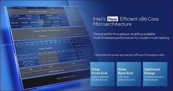
That is just the surface specifications as once you dig into them you realize that Intel has hot rodded them over previous Atom designs. Most blatant of all changes is Gracemont is the first to support AVX2 and even AVX-VNNI (Vector Neural Network Instructions for AVX). It even has 17 execution ports instead of the 12 in previous designs (though we doubt it is physically able to do 17 instructions concurrently). Beyond that however, Intel has bumped up the buffer size and buffed its capabilities. For instance, the reorder buffer size is now a whopping 256; instead of 64KB (32KB data + 32KB instruction) per core of L1 cache each of these have 96KB (64KB instruction + 32KB data) L1 Cache. Each 4-core block / module also has access to a shared 2MB of L2 cache… and most importantly of all the e-cores share the same 30MB L3 cache pool as the p-cores.
