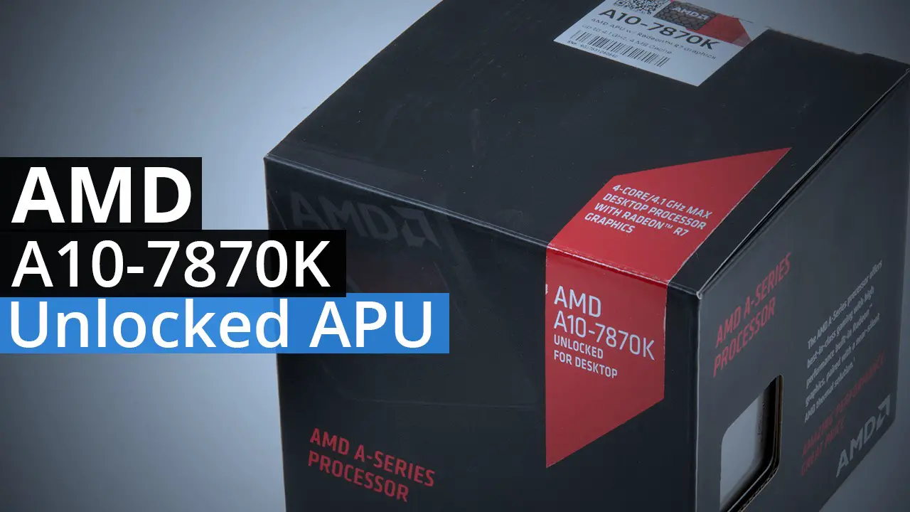
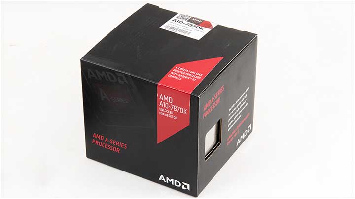
 As with the A10-7890K review (which you can read here: AMD A10-7890K) the best place to start is describing exactly what an ‘APU’ is and how the A10-7870K is designed. Firstly, an APU is an Accelerated Processing Unit and basically is a CPU (Central Processing Unit) with an GPU (Graphics Processing Unit) built right on to the same piece of silicon (aka ‘on-die GPU’). However, this does necessarily mean a larger number of pins are required. To be precise AMD’s FM+ APU’s use a 906 pin design (with the pins being on the APU and not the motherboard’s socket) instead of 941 pins AMD’s AM3 processors require.
Now AMD has been designed APUs for quite some time now and to be precise the A10-7870K is a fifth generation APU (codenamed Godavari) and is the second generation APU to be built using AMD’s Heterogeneous System Architecture (HSA). As we saw in the A10-7800 review (AMD A10-7800), HSA does make a difference and does allow core components that date back to early 2014 to compete with Intel 2016 designs… and win on the video front and overall value front – while doing a darn decent job on the CPU front as well.
So what is a Godavari APU made up of? Basically it is the same as a A10-7850K but at higher clock rates. This means two CPU blocks for a total of four Steamroller based Compute Units running at a maximum speed of 4.1Ghz. For the ‘GPU’ portion of the core the A10-7870K has eight video Compute Units. These eight graphic Compute Units are based on an R9 2-series design, and run at 866Mhz while still boasting 512 stream processors, 128 Texture Units and all the other sundries that make up a modern AMD 2-series R-7 ‘GPU’.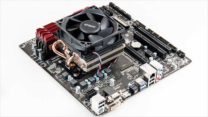 Also as expected to make all twelve of these Compute Units work together as one cohesive whole AMD’s HSA layer resides ‘on top’ of them. This in turn means the four CPU Compute Units can create and send work directly to the eight video CU’s and vice versa (via what AMD calls heterogeneous Queuing, and the industry simply calls Dynamic Parallelism). Better still this cross flow of GPU calling on CPU functions (and vice versa) is all done at the kernel level and does not require OS, API, or even drivers to do so. Instead it is bare-metal crosstalk that is a lot more efficient than a discrete CPU and GPU… or even an older APU’s ways of doing things.
More importantly is the twelve cores now share the entire RAM amount as one large memory unit instead of dividing it upon POST into two parts… that could not be shared or even ‘seen’ by the other Compute Unit type. This is called hUMA (heterogeneous Uniform Memory Access) and works darn good and requires a lot less TLC than the old way of dividing and hoping one type does not run out of memory. The works loads are also now equally spread across all the CUs and each CU knows what the others are working on so as to not cause issues with writing to memory sector that another is reading (‘Platform Atomics’).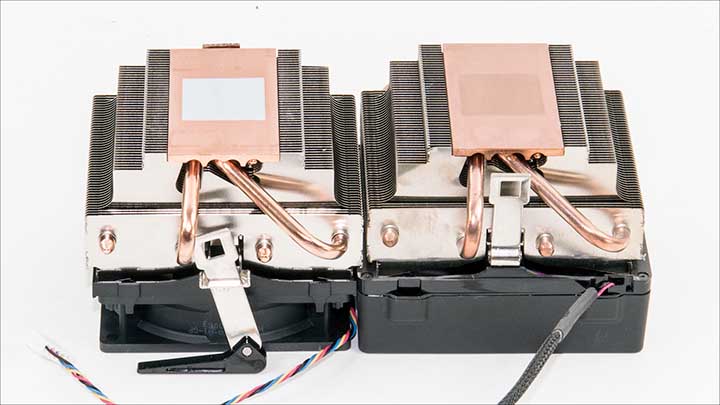 Also noteworthy is just as with the A10-7890K, the A10-7870K is a ‘black’ processor. In layman’s terms this means it is an unlocked processor that allows for rather easy overclocking of both the ‘CPU’ portion and the ‘GPU’ portion. In testing we easily pushed the four CPU cores to 4.5Ghz and pushed the GPU cores to 1040Mhz. That is damn impressive considering we did all that and still did not hit the 72-degree thermal wall. Needless to say the Near Silent CPU cooling solution may not be quite as good as the 7890K’s ‘Wraith’ but it still is more than capable of cooling this APU even when overclocked. This does make sense as it basically is a Wraith just with a lesser performing fan attached!
