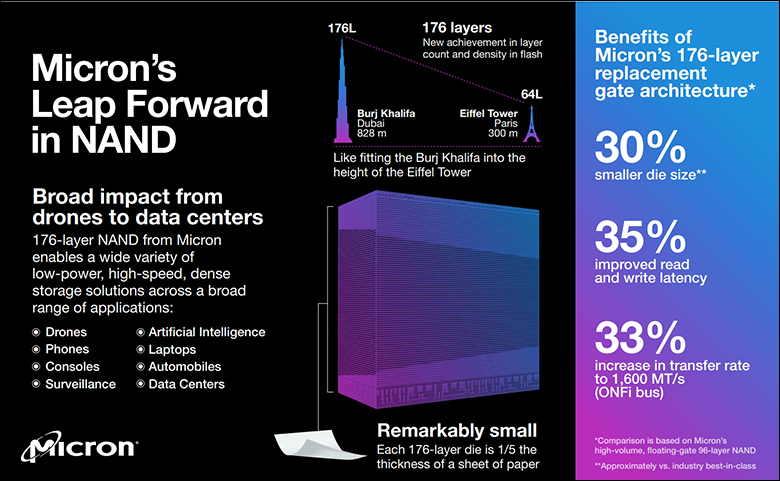
For those that have read our previous Solid State Drive reviews the easiest way to imagine what Micron has done in order to create their ‘Replacement Gate’ NAND is to imagine the melding of typical Charge Trap design with earlier Micron CuA NAND logic layout. Then imagine it bigger, stronger and better than other NAND designs available on the market today. Simply put, it is a new spin on Charge Trap NAND theory and design… and not an entirely new approach to NAND design.
For those that are new(er) to SSD technology and want to know exactly what ‘Replacement Gate Technology’ is… a bit more theory and information is needed. The foundation of all Not-AND (aka ‘NAND’) Solid State storage is a tiny little electrical gate, and a tiny little electrical ‘battery’ cell called a transistor. To change the stored data bit from a 0 to 1, or vice versa, the controller tells the gate to either let the charge ‘out’ (aka ‘discharge the cell’) or store some in the cell. This is called a program operation as it is literally setting the charge state of cell or ‘programming’ it.
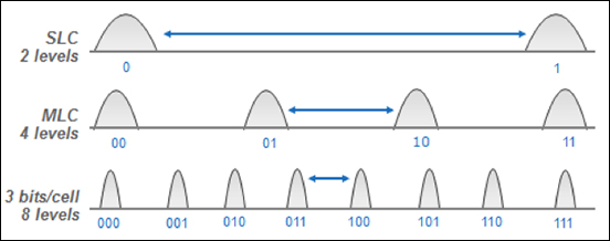
To read the NAND cell the controller simply pushes a tiny trickle of power across the gate and reads that cell’s charge. For example, in SLC or single level cell NAND the cell has two states: full and empty. Ironically, since the controller is reading a difference in voltage across the cell, the default ‘empty’ state is usually considered 1 and not a 0. So, an ‘empty’ or discharged state is the same as storing a 1 in that cell, and fully charged is a 0 bit. For old timers, this is why in AS Cleaner or ‘Tony Trim’ type programs (before TRIM was a sure thing) you had to use the ‘FF’ write option… as ‘FF’ is the same as all ones being written to the cells.
Since a NAND transistor can hold its charge even when the system is powered off, NAND storage is considered ‘non-volatile storage’. However, just like ‘bit rot’ on a Hard Disk Drive this state is not permanent. Instead, and just like the battery in your turned off phone, if left long enough the power in those tiny transistors will leak out… and turn a 0 into a 1. This is a bad thing from a long-term storage point of view.
With SLC NAND, a cell that is left alone will not lose all that much voltage and is fairly stable for months between power on states. However, as each NAND cell can only store 1 bit it is rather expensive to create say a 1TB Solid State Drive, and scaling up beyond 1TB requires a lot of NAND chips. Even layering NAND cells on top of NAND cells on top of NAND cells the resulting footprint would be rather large. This combination is why Multi-Level Cell NAND was created and doubled a NAND cell’s storage capacity from 1 bit to 2 bits. It did this by adding more voltage resistance points between ‘full’ and ‘empty’. So instead of two states there was now four states: 0, 0.25, 0.5, 0.75, and 1. This certainly increased storage density, and decreased cost of manufacture to hit a given storage capacity, but at the same time made the self-discharging of NAND a greater issue – as lot less of a voltage change can indeed impact two bits of data. This is why MLC is not as stable as SLC and has to be refreshed / rewritten more often (aka ‘internal housecleaning’).
As time went by MLC was further supplanted by TLC (Tri-Level Cell) NAND which can store three bits of data per cell. In TLC NAND there are not two, not four, but eight voltage states (for comparison’s sake to hit 4 bits per cell, QLC NAND requires sixteen voltage points). This in turn increases the necessary precision in properly writing and reading a given state of a NAND cell. It also significantly decreases how long a TLC NAND cell will hold this more precise voltage state. This increased precision plays a large role in why TLC NAND is ‘slower’ at write operations than MLC (which is in turn slower than SLC).
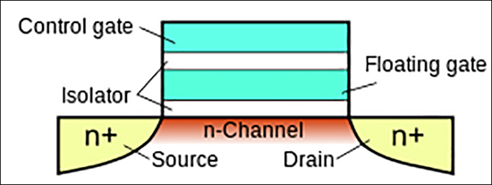
In original NAND design how a NAND transistor worked was via a ‘floating’ gate (FG for short). With an FG transistor the gate itself is the conductor of electricity. Thus, in order to change a NAND cell’s state electricity must be pushed through the gate itself. Over time this sudden shock of current running through the floating gate causes miniscule fractures in the crystal lattice that makes up its foundation.
The size of these fractures and their likelihood of occurrence is directly tied to how hot the transistor is; however even a ‘cold’ NAND transistor will do slight damage to its gate every time a charge state change is required. On their own a single fracture will not cause voltage related issues, but over time the culminative effective does create a significant problem. When this happens, the end result is a gate which is incapable of keeping voltage levels inside the transistor stable. This is what a ‘dead’ NAND cell really is – a NAND cell that can no longer be trusted to hold a precise charge.
Worse still, with every reduction in fabrication node size the cell itself not only becomes smaller but the gate itself also becomes smaller. A smaller gate not only has less tolerance for heat but means fewer defects are required before the gate fails. Also, the more precise the voltage requirements the faster accumulative defects become an issue.
In laymen’s terms, a floating gate literally ‘eats itself’ every time it is called upon to change the charge state of its transistor(s). The smaller the gate, or the more precision required, the faster it finishes its meal… and the faster the cells die. NAND manufactures are aware of this issue and include free NAND cells to replace ‘dead’ cells. They are also fully aware that this is only a band-aid solution as eventually there will be no more replacement cells left.
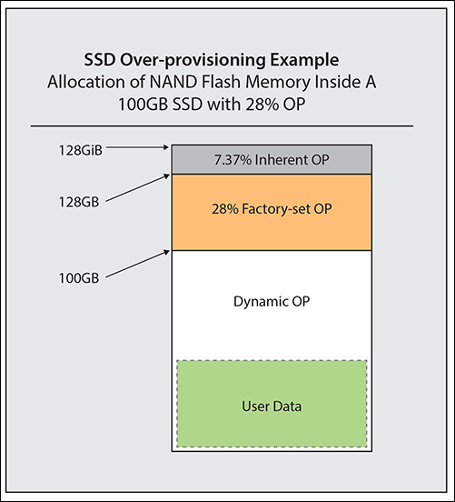
Controller and storage companies are also aware of this issue and include even more ‘replacement cells’ (aka ‘over-provisioning’ and why your 256GB drive may be seen as a 240GB drive) but also use slower / gentler write algorithms to reduce this damage (typically 8 voltage steps or more). In simplistic terms this means they write to the NAND using less voltage but over a longer period of time. This does reduce cell damage, but at the cost of write performance. To overcome this side effect, the controller will pretend a given chunk of TLC NAND is SLC NAND and only store two charge states instead of eight (or 16 in the case of QLC) per cell. This allows those cells to continue being used long after the amount of damage to the gate would result in random bit changes if eight (or more) states were needed. This pseudo-SLC is then used for real time writes as a buffer and is called different things by different manufactures. For example, Crucial calls it “Dynamic Write Acceleration”.
Sadly, including more backup NAND cells and / or lowering the voltage applied does nothing for charge coupling. This rare event happens when the fracture is close enough to a neighboring NAND cell that the electrons can jump from one cell to another creating a quasi-bridge between the cells. This in turn can randomly impact multiple cells worth of data and do so silently – with the controller only knowing about it when it checks the state of the cells vs. what they were supposed to be. To visualize this imagine sorting your spare change into cups that are touching one another… and a quarter bounces off the lip and ends up in the dime cup. Both cups total amount will be off, and you will not know they are off until you count both cups.
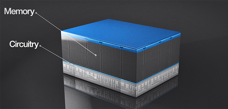
These are all well-known issues. Issues that have been known for decades. While Samsung and Toshiba opted to change the very foundation of how their NAND transistors work… Micron and Intel opted to increase the size and rearrange their cell layout to help reduce them. Put another way, they decided to kick the can down the road. The upside is the CMOS under Array (CuA) design was created. One where the interconnects are much like ‘elevators’ in an apartment building (at the ends of the ‘hallways’) and the logic hardware is under the NAND transistor array (think ‘basement’ in an apartment building). This layout helps (to somewhat) alleviate heat buildup by moving the potential hotter running interconnects closer to the edges of the NAND block.
The downside to typical CuA NAND is twofold. Firstly, it was still FG tech based. Secondly, CuA is not exactly the most efficient layout. It does have a tendency to bottleneck slightly faster than some of the competition… and the deeper the NAND layer depth the more it is likely to occur under sustained extended loads. To help minimize this last issue, Micron has opted for a rather fast ONFI “NV-DDR3” rev 4.2 bus which can handle 1600 Mega Transfers per second. Thus CuA “Replacement Gate” has ‘hallways’ and ‘elevators’ which are 50 percent wider than the previous CuA NAND’s 800MT/s bus. This works rather well at alleviating the pressure and keeping performance in tip top shape… even under extreme conditions. Will that still be the case in the future when 200+ Layer NAND is created? No one knows. What Micron is betting on is that ONFI will to continue to increase the spec’s speed faster than their CuA’s low-level bottlenecking issue. Considering ONFI 5 standard calls for another 50 percent increase in performance (2400MT/s) time will tell if their gamble pays off or not. In the meantime, their existing Replacement Gate NAND tech is relying upon an incredibly fast bus (by today’s standards) that is more than up to the demands placed upon it.
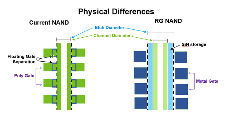
This is where the other half of the changes that come along with Replacement Gate technology come into play… as Micron literally replaced their NAND cell’s gate technology. Instead of the Float Gate that was used before, and all the issues outlined above that go along with it, Micron has finally admitted that Charge Trap (CT) design is superior. Since Intel is essentially out of the consumer marketplace this makes Float Gate design a dead tree branch tech. One that only CompSci university students will learn about in their history books.
In CT based NAND, the gate is not a conductor, instead it is the insulator. So instead of being responsible for getting power into the gate, it is responsible for keeping it there. This means during write or erase operations less stress is being placed on the gate itself. Since the method of charging/discharging is different the operation can not only be faster (typically about half the time vs FG) but gentler (typically 6 voltage states). The end result is those deadly fractures are less likely to occur, and when they do happen they are usually measured at the electron level. Since they are smaller, they can only drain off the electrons that are ‘touching’ the fracture. Leaving the rest of the electrons in the cell to control the voltage adequately enough that the controller can still accurately tell what the cell state is.
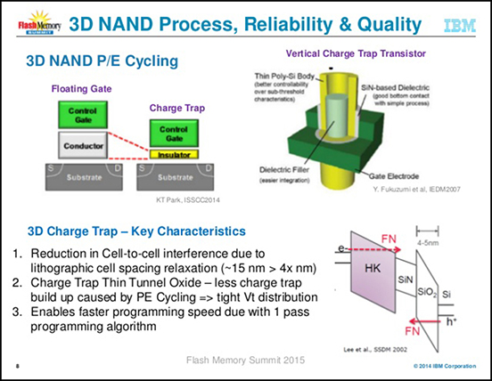
While yes eventually fractures in the gate’s lattice matrix will multiply to the point that they too also cause the cell to be marked as ‘dead’, the likelihood and severity means a CT based NAND transistor will last noticeably longer than float trap design. Equally important, this in turn not only increases longevity of the NAND cell but also allows for faster – and yet ironically enough still gentler- programming cycles to be implemented on the NAND. Which in turn increases sustained write performance. Charge Trap gates also gain longevity and performance from the switch from planar (aka 2D) NAND designs to 3D designs. Arguably CT NAND gain even more durability as they do not ‘eat themselves’ nearly as fast as FG NAND – so the increased mass means the NAND cells last even longer. When paired with pseudo-SLC algorithms the end result is higher sustained performance, increased durability, and generally a better end-user experience.
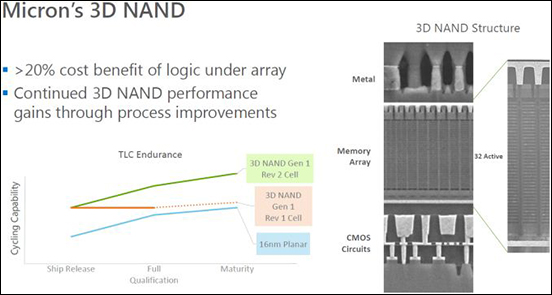
Where Micron was starting with both a blank slate and over a decade worth of real-world data provided to them by their competition their design team has been able to focus in fixing a weakness that existing CT designs have – their layout. In classical Charge Trap NAND each cell is basically laid out just as it would be in FG NAND design, with each cell being a sperate and distinct ‘apartment’… with one ‘family’ (or 1/2/3/4 bits of storage depending on NAND type) per ‘apartment’. While this is indeed an improvement in both the durability and performance characteristics; charge coupling is still an issue, performance is still not optimal, and neither is data density.
To understand these issues, imagine the typical high end condo building. While all the condos on a given floor share the hallway, each condo has its own door and rather thick “firewalls” separating one condo from another. In Replacement Gate technology… Micron has clustered cells into groups. With a nonconductive layer of silicon nitride surrounding the insulator gates. This not only allows for increased performance (~35 percent over their previous gen), but a noticeable reduction in footprint (this 176Layer NAND takes up about the same room as their 64Layer FG NAND did). It also promises to be even more resilient to charge coupling issues – further making it even more reliable – when compared to standard CT NAND designs. These promises remain unknowns and only time will tell if Micron has indeed created a better design, but it certainly shows potential.
Without going into white paper levels of detail all the above is the simplified basics on what makes Replacement Gate Technology ‘tick’ and why Micron has indeed not only achieved parity but arguably surpassed the competition.


