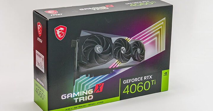
This is where the large, pink tutu wearing, elephant enters the equation. To be blunt, NIVIDA may have been a touch optimistic on how much more powerful their new Ada Lovelace architecture really is. Yes, it is bloody efficient. Yes, they “rebalanced” the memory arch’ to give their L2 cache starved cores a good chunk (32MB in the AD106-350’s case) of extra memory. Yes, this does reduce the number of times the RAM buffer has to be accessed compared to previous generations.

Sadly, counter acting all those wonderful improvements is NVIDIA actually reduced the number of CUDA cores from 4864 to 4352 (i.e. 512 are “missing”). Reduced the Ray Tracing cores from 38 to 34. Reduced the Tensor cores (aka DLSS cores) from 152 to 136. Then if all that was not enough, they cut the memory bus in half. Yes. Poof. Gone is that lovely 256-bus the 3060Ti and the 2060 Super (aka Ti for the Ti’less generation) had. Hell, even compared to the 1060 Ti and its 192-bit wide bus , 128-bits is teeny tiny. It ‘feels’ like a x50 bus… as the 3050 Super used a 128-bit bus.

Why did NVIDIA do all this? They did it due to the Ada Lovelace architectural design and philosophy, expected demand for the 4060 and 4060Tis… and how incompetent Samsung’s 8nm fab division are compared to TSMC. That second and third bits are getting ahead of ourselves. Instead let’s rewind the clock to when NVIDIA were making Ada Lovelace a reality. Specifically, they were designing the AD102 ‘grand daddy’ that is base blueprint for all the smaller AD10x-series (consumer) cores. Regardless of the model, all ADA’s are made up of key building blocks called Graphics Processing Clusters (GPCs). A “GPC” consists of up to 12 Ray Tracing cores, 48 Tensor cores, and 1536 CUDA cores that are active… and is paired with a single 32bit memory controller. In the AD102-400 (aka RTX 4090Ti) that means the (nearly) fully monty of (nearly) 12 active GPCs, and 12 memory controllers… for a grand total of 142/568/18176 goodness with a 384-bit bus capable of handling 24GB of RAM.
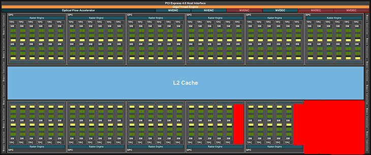
Slice off 4 GPCs, and then disable 1 and then either 1/6th in two GPCs or a third in one GPC (6 + 2/3rd GPCs active) and you get a AD103 “RTX 4080” with a “only” 80/320/10240 goodness but on a 256 bit bus… with room for a “fully enabled” RTX 4080 Ti for later release (8 GPCs active).
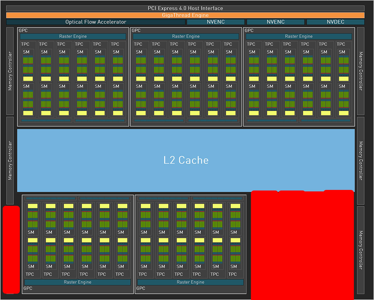
Slice off the deactivated GPCs and another full GPC in the AD103 (for a grand total of 5 fully enabled GPCs) and you get a AD104 “RTX 4070 Ti” which gives us our oddball 192-bit buss (5x32bit memory controllers) and 60/240/7680 cores.
Cut one full GPC and 1/6th of another (3 full GPCs + 5/6ths of a fourth GPC) and you get an AD104-250… aka GeForce RTX 4070. Which keeps the 192 bit bus, but drops down to 46/184/5888 cores.
In a (slightly more) “perfect” world NIVIDA would have then taken the AD104-250 and laser cut that remaining 5/6ths of a working GPC to make the foundation for their RTX 4060 Ti and then laser cut some more for their RTX 4060. Sadly, x60s (and x60 Ti) are arguably the most popular of NVIDIA’s consumer GPU lineup every generation. So using failed chips would have caused “production issues”… with NVIDIA forced to laser cut factory sellable AD104-250’s to get the numbers needed for their RTX 4060 and 4060 Ti cores.
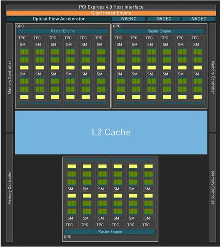
This in turn would have given their (leather jacket wearing) MBA’s hives when thinking about all those modified RTX 4070 cores being sold as lowly RTX 4060s. Which is ironic as previous generation did basically that and NVIDIA made record profits. Yes. In the RTX 3000-series the GA102 variant was used in RTX 3090Ti/3080Ti/3080… and even some 3070 Tis (when necessary to get rid of failed chips). Then a ‘small core’ GA104 was used for RTX 3070Ti/3070/3060Ti/3060 cores. Thus, the 3060Ti’s being allowed to have 256-bit bus. Which is impossible on the Ada Lovelace design as it stands today. One could argue this is because NVIDIA did not want to waste working chips like they did in the RTX 3000-series heyday, but it is more a case of Samsung’s 8nm production line being so incompetent that NVIDIA had to pivot to make use of all the “mostly working” cores coming off each wafer… versus TSMC actually being good at their jobs and delivering on what they contracted to deliver.
