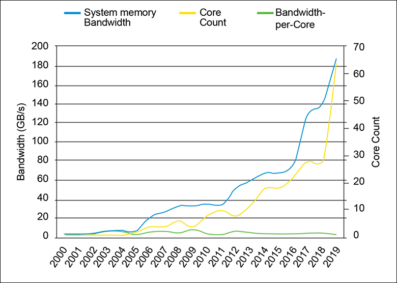
Why do such changes matter? They matter because the memory bus can not only move noticeably more data per clock cycle, but it can also be much more efficient at what it moves per cycle. This, in turn, means each CPU core spends less time waiting for the off-chip cache data it requested. This “less filler, more killer” approach to data transmission wouldn’t mean much if we were dealing with 1, 2, or even 4 cores. Those days are also long in the past. Thanks to the ongoing “core wars,” consumer CPU core counts have ballooned while memory bandwidth (and capacity) per core has not. Thus, in the future, efficiency per cycle will arguably be just as—if not more—important than sheer speed. That’s why there are a bunch of other tweaks baked into DDR5, and we’re only hitting the highlights. So much so that DDR5 is a (relatively) radical departure from previous JEDEC standards. A standards body known for its ultra-conservatism and reluctance to make major changes unless they are forced to.
These low-level improvements are also why DDR5 officially starts at 3200 MT/s… but in reality, DDR5-4800 is the true baseline (aka 2400Mhz aaka 4800MT/s aaaka 38.4GB/s aaaaka PC5 38400). Speeds then officially climb to 6400 MT/s (aka DDR5-6400 aaka 3200MHz aaaka 51GB/s aaaaka PC5 51000… that’s too many alternative ways of saying the same thing). That’s the situation right now. DDR5-8400, ticking along at a whopping 4200 MHz, is already viable, and assuming DDR5 has the “legs” DDR4 had, even higher frequencies are possible—maybe even likely.
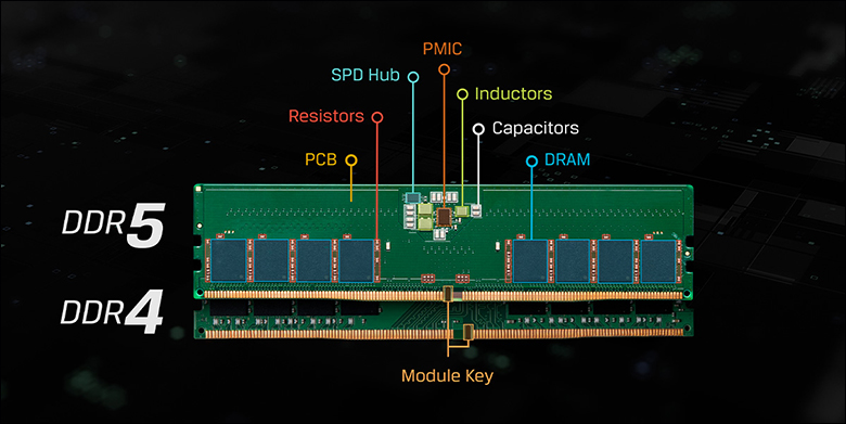
In either case, to put those numbers in perspective DDR4 clock frequencies are typically 1066.67 (DDR4-2133) to 1600Mhz (DDR4-3200)… with some extreme examples above that like 2000MHz (DDR4-4000) and even DDR4-5000 (2500MHz). Which are indeed real and (technically) viable options… if you A) have the money (and the upper end of DDR4 makes similarly clocked DDR5 look cheap in comparison) and B) have a golden CPU with a golden IMC capable of handling those insane (for DDR4) clock rates.

On its own, speed and efficiency are all well and fine, but it’s when you look at ECC (error correction code) that you see another massive sea change in how data is stored and secured. DDR4 offered channel (aka sideband) level ECC. It was optional, not standard. It achieved this by widening the bus from 64 bits to 72 bits, with the extra eight being used for ECC. It required a memory controller capable of handling ECC (few consumer-grade CPUs could), BIOS support, and special DDR4 memory that supported it. Put another way, DDR4 ECC was expensive—expensive and rare enough that it was mainly sold and used in enterprise-grade hardware.
DDR5 changes all that. With DDR5, every single DIMM comes with on-die ECC. As the name suggests, on-die ECC is ECC baked right into each DIMM’s IC, with error code correction being created and stored right along with the data being written. In (extremely) simplistic terms, JEDEC (Joint Electron Device Engineering Council) took a page from modern solid-state drives and added 8 bits of ECC for every 128 bits of data written. To imagine this, think of a group of hard disk drives in a RAID array: each HDD writes the bits and bytes to its platters, then adds a parity stripe to secure that data and ensure integrity even if a drive fails. If, during a read operation, the data doesn’t match the ECC parity stripe, the data is corrected before reaching the end user. That parity stripe is basically the same idea as the on-die ECC DDR5 uses.
This analogy, however, is a gross oversimplification.
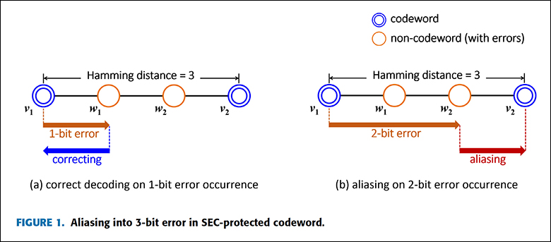
DDR5’s ECC is Single-Bit Error Correction (SEC) with (technically) dual-bit error detection ECC (via an extra parity bit). Yes, Samsung has used it in the past. Yes, it’s better than nothing. It is, however, certainly not true SEC-DED (Single-Bit Error Correction with Double-Bit Error Detection), let alone legitimate SECDEC (Single- and Double-Bit Error Correction).
We say this for many reasons, but the main one is that, unlike in our RAID analogy, when an error is detected, the ECC does not fix the data in the RAM cell array right away. Instead, it simply sends the corrected data down the pipe without issuing a rewrite request for the 128 bits of erroneous data. It does not automatically correct errors because DDR5 includes an ECS mode (“Error Check and Scrub”) that occurs roughly once every 24 hours, leaving a known bad bit in play for up to a full day. This extended period between when data is known to be bad and when it’s fixed dramatically increases the chances of a double-bit error occurring.
We understand why it was implemented this way; we just disagree with the notion that adding an extra 135 bits’ worth of writes in real time would negatively impact performance enough for anyone to notice. Thankfully, even when operating with known-bad data, a single-bit error remains a theoretically rare event. Making any ECC in consumer-grade RAM overkill by its very nature. Overkill enough that it hardly justifies wasting capacity or cycles on more computationally intensive ECC capable of double-bit error correction.
Along those lines, this ECC also only fixes errors that happen inside the ICs. It does nothing and can do nothing to protect data integrity once it leaves the DIMM. It doesn’t even protect data from being corrupted on the way to the DIMM. Considering RAM IC-level errors (mainly due to thermal and voltage leakage–related bit flips) are where most errors arguably occur, this 128+8 SEC protection is still a major improvement. It just isn’t a silver bullet, nor should it be considered one. A cynical person might say it was simply added to allow memory manufacturers the luxury of loosening production standards, as the ECC will or should catch any real-world errors. That’s a bit too cynical for us, but the reason doesn’t really matter all that much. Some ECC is always better than none, and it represents a major change in JEDEC’s priorities.
Of course, while the ECC baked into the DDR5 standard is not end-to-end protection, DDR5 will also come in a “DDR5 ECC” flavor. This now-secondary “sideband” ECC has also been improved, with each subchannel using a full 8 bits of ECC (i.e., 32+8 transmission). So it’s 72 bits vs. 80 bits—or twice the amount of ECC. The more ECC bits, the more fine-grained and robust the protection can be… the more it can “fix.” Furthermore, this combination of sideband ECC plus in-die ECC will provide protection from the moment the data hits the memory controller until it’s stored in the RAM (and vice versa). Just don’t expect this OCD level of “end-to-end protection” to be cheap… as it will still require a memory controller capable of sideband ECC and DDR5 ECC kits and… and… and.
