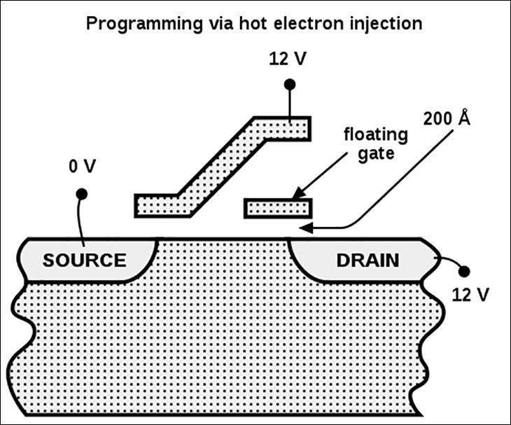
Before we being get to the P1 we should start with a short primer on NAND and how it is uses to store data. NAND or Not-AND floating gates are small little gate resistors that either allow electricity flow through them freely or block it. When a controller wants to store a 1 it gives the resistor a tiny trickle of power to change the gate state so that power flows easily through it. To turn a 1 into a 0, it changes the gate’s state so that electric cannot flow past the gate. To read a NAND cell the controller pushes a small(er) trickle of power through the gate and reads the voltage level it gets back. If it gets back what it pushed through the cell it’s a 1, if it doesn’t get anything back it’s a 0. Pretty simple right?
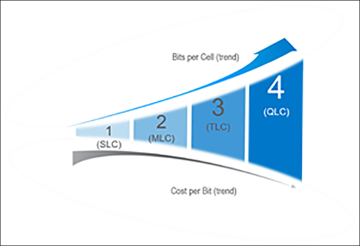
Well yes and no. This Coles Notes version is on how things used to happen when the NAND cell was only expected to store one bit of data. This was Single-Level Cell NAND. Then came Multi-Level Cell NAND which could store 2-bits per cell. It did this by adding in a level of complexity to a rather simple idea. Instead of a cell either passing electricity or not… it had to have four states. 0, .25, .5 , .75, and 1. Then came 3-bit NAND (Tri-Level Cell / ‘TLC’ NAND). This NAND requires not six but eight voltage levels. To add another bit – for a total only four bits per cell – there has to be sixteen possible voltage return states.
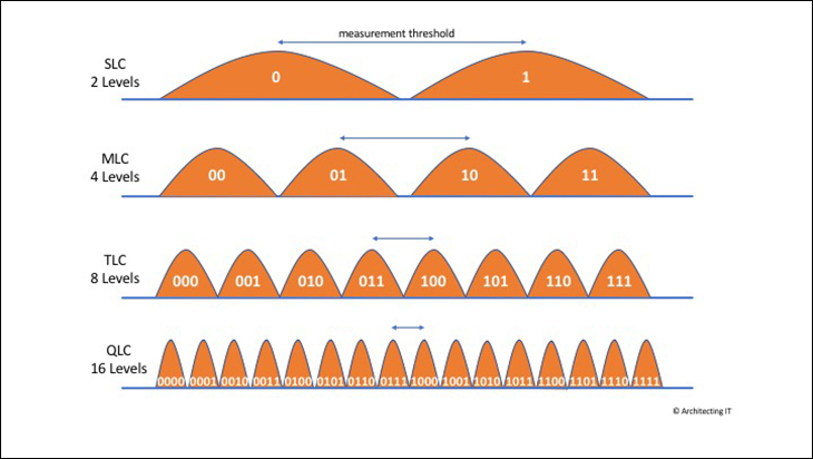
Every time the number of voltage states increases the ability to read and write to the NAND becomes harder and harder as the controller has to be more and more precise. Which in turn makes it a slower and slower process. Worse still, from a performance point of view, the ability of the NAND to keep the proper state becomes harder and harder as the number of voltage states goes up. Remember the difference between a 0 and 1 in one of the four bits is only 1/16th of a voltage state. Basically, with QLC very little damage to cell can cause the voltage to ‘leak’ past the gate and turn what was supposed to be a 0 into a 1. This means the controller has to use a much gentler write process that takes longer to accomplish… as otherwise it will harm the NAND in short order.
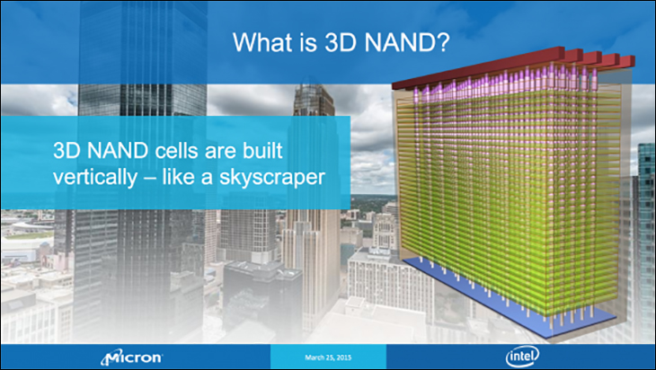
So what does this mean to you the buyer? It means that manufactures had to come up with ways to boost performance and durability if the NAND revolution was to continue steam rolling over hard disk drive technology. The first solution was to go to ‘3D NAND’. This allowed the manufactures to make bigger cells and still increase capacity per square millimeter. The bigger the cells the more damage it can take before ‘leaking’ makes a cell unstable – boosting durability. This also somewhat helped to boost performance higher as the controller does not have to be as delicate on the NAND during writes as it did with 2D or planar NAND cells.
Mainly though, the way in which they improve performance is via a catch-all term called ‘pseudo-SLC’ or ‘pSLC’ write buffer technology (the term varies from manufacture to manufacture with Crucial calling it Dynamic Write Acceleration). What this means is simple to explain but is rather complex to accomplish. The controller pretends that MLC/TLC/QLC NAND cell does not have more than two states… and instead treats it as a rather large and complicated ‘SLC’ NAND cell. Since the pretend SLC NAND only has ‘two’ states it is nearly as fast and efficient to read/write from these pretend cells as it would to ‘real’ SLC NAND cells. It is also a heck of a lot easier on the cells themselves. This in turn boosts performance and durability well beyond what was thought possible before pSLC came on the scene.
The downside is two-fold. The first is each bit of this write buffer requires four bits of storage capacity. So in order to have even just a piddly little 1GB SLC write buffer… requires 4GB of space, and 100GB would take up a whopping 400GB of capacity. The other is that performance is variable on drives that use a ‘pSLC-write buffer’. Once this buffer is filled the controller has to first empty it before it can be used. This means that while it is emptying the buffer to the rest of the NAND cells on the drive, the controller also has to write directly to the slow TLC/QLC NAND. Meaning performance and cell longevity tanks. This is why manufactures want to use as big a write buffer as possible, but it is a delicate balancing act. Too big means the price per Gigabyte of storage goes back to SLC prices. Too small… and performance goes back to hard disk drive levels. This happens with SATA based models. It happens with NVMe. It happens with MLC NAND. It happens with TLC. It happens with QLC. It just is with NVMe the disparity is rather jarring to say the least, and only gets worse the higher the bit depth per cell gets.
This is why some models like the Crucial P1 use a hybrid approach to pSLC size (or what Crucial calls ‘Hybrid-Dynamic Write Acceleration’). What this means is the pseudo-SLC write buffer’s capacity varies depending on how much free capacity there is available but the minimum size has been hard set to ensure there is always a pSLC buffer no matter how full the drive is. In practical terms this means the Crucial P1 1TB has massive 140GB buffer when the drive is empty, a 75GB or so pSLC buffer when half full, a 25GB when the drive is at 75% capacity, and when nearly full only 12GB (as this is the minimum the pSLC can shrink too on the P1 1TB – on the 500GB P1 the minimum is only 5GB). Keep this in mind when thinking about how big a drive to purchase and looking at TLC and QLC based models. When in doubt… go bigger than you think you need. Considering long term storage, or the buffer is filled. This in turn does further increase NAND endurance, extend the time between having to ‘refresh’ the data via re-writes, and reduces the chances of data loss during power loss. Remember this series is a M.2 based form-factor drive and there is simply no room for capacitors on the PCB. So the less data that is being moved to-and-fro the better. Instead only the data in the short-term RAM buffer is at any significant risk. Crucial does use the usual SMI algorithms to minimize this risk and all told it is a very elegant solution to both data integrity and endurance. Most likely such a configuration is the future for TLC NAND drives and not just QLC… as these refinements do have a way of ‘trickling down’ to models that don’t even use the NAND type they were originally designed for.
