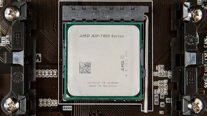
The AMD A10-7800 represents the fourth generation ‘APU’ design that AMD started back in 2011. That first generation was called ‘Llano’ and was basically two discrete processors crammed on to one piece of silicon (a CPU and a ‘GPU’). Then came the original Trinity which helped boost performance; then there was ‘Richland’ that showed AMD was serious about performance. They were still basically two discrete designs on one ‘processor’ and not really a true Accelerated Processing Unit.
With Kaveri, AMD has changed things up and created what they call a Heterogeneous System Architecture (HSA) that melds bot the CPU and GPU into one true single architecture. In simplest terms what this means is that both the CPU cores and GPU cores can interact much more efficiently with each other, require less power to hit a performance goal, and can even have their TDP modified by the end user!
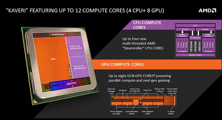
In order to make a homogenous – or heterogeneous – design AMD took a page from their Video Card division and created basic building blocks upon which the full processor will be built. Much like a modern AMD video card processor these compute ‘modules’ or ‘units’ are the building blocks upon which the ‘real’ processor is built. To make a smaller, lower power model AMD simply uses less… and for more powerful models they use more. These compute units come in two ‘flavors’: CPU and Graphics… and it is fairly self-evident which does which. Along with this change AMD has changed their terminology and now there is not ‘cores’ and rather it is Compute Units. In the case of the A10-7800, it has four CPU Compute Units and eight graphics Compute Units…. or a twelve core processor.
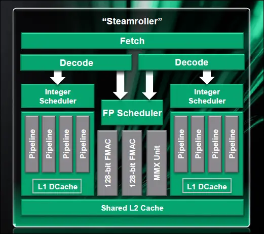
Let’s break this down, and how AMD arrived at this final design. The A10-7800 has two CPU building blocks and one GPU building block. Each of the CPU building blocks is a Steamroller based design that allows for two simultaneous threads. To be specific each of these CPU building blocks has its own L2 cache, one shared floating point core, two integer cores, as well as its on decode and fetch hardware to access the external cache, and even the RAM. Since there are two integer cores AMD calls this a dual compute unit… and not a triple like they do with their CPUs (as AMD calls the shared floating point another ‘core’). Interestingly enough Steamroller is a refreshed and refined version third generation X86 Bulldozer architecture – though with a lot of improvements, so many AMD states a 20% clock for clock improvement over the second generation. Since there are two of these blocks, this how the A10-7800 has four CPU Compute Units.
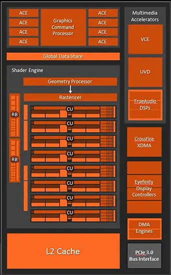
For the graphic’s building block, AMD actually used their – for the first time – GCN GPU architecture to create it. Much like a AMD R9 290 video card that it is based upon the GPU module features up to eight Asynchronous Compute Engines (ACE) and up to eight GPU Compute Units. In the A10-7800 case there are eight of these graphics CU’s. As with a R9 2-series each of these gaphics CU is made up of 64 stream processors and 16 Texture Units. Giving the A10-7800 a grand total of 512 stream processors and 128 Texture Units… plus all the other low level goodies that make an AMD video card processor a AMD video card processor. That is a lot of video processing power for a processor!
Now all this is fairly typical for how AMD did a APU in the first three generations – albeit with a lot of tweaks and the like – but what makes the Kaveri APU generation so special it is the additional HSA layer that melds the two into one true mega-core.
This in turn means the four CPU Compute Units can create and send work directly to the eight video CU’s and vice versa (via what AMD calls heterogeneous Queuing, and the industry simply calls Dynamic Parallelism). Better still this cross flow of GPU calling on CPU functions (and vice versa) is all done at the kernel level and does not require OS, API, or even drivers to do so. Instead it is bare-metal crosstalk that is a lot more efficient than a discrete CPU and GPU… or even an older APU’s ways of doing things.
More importantly is the twelve cores now share the entire RAM amount as one large memory unit instead of dividing it upon POST into two parts… that could not be shared or even ‘seen’ by the other Compute Unit type. This is called hUMA (heterogeneous Uniform Memory Access) and works darn good and requires a lot less TLC than the old way of dividing and hoping one type does not run out of memory. The works loads are also now equally spread across all the CUs and each CU knows what the others are working on so as to not cause issues with writing to memory sector that another is reading (‘Platform Atomics’).
