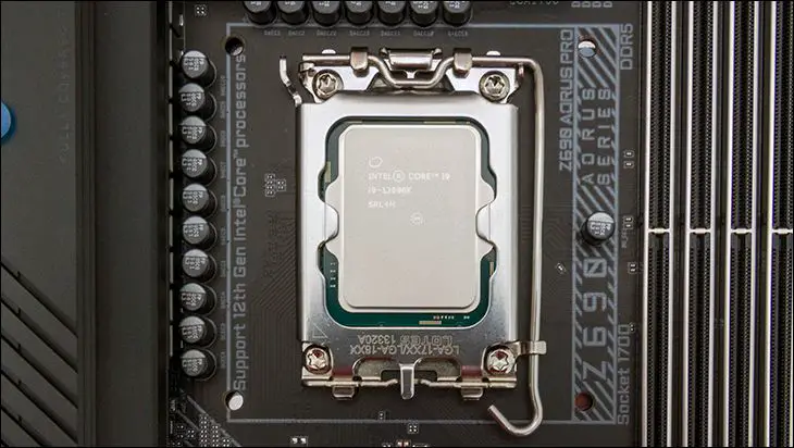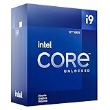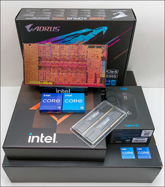
Where we are privileged to have received the limited-edition reviewer’s box o’ goodies we cannot comment on the shipping container retail buyers will get. Instead, ours came in a small box… inside a bigger box… inside an even bigger box. The same holds true of accessories. Intel might be hungry to take sales away from AMD, but even Core i9 buyers will never get their pick of either a ‘free’ Asus ROG Maximus Hero or Gigabyte Aorus Pro Z690 motherboard… and have Intel throw in a Logitech mouse to sweeten the deal. What we can firmly state is this swag, while nice, did not sway our final opinions one way or the other. We simply consider them a nice little bonus.
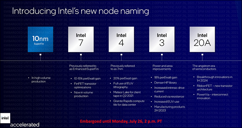
As is our typical Modus Operandi let us start with the most obvious changes between Rocket Lake (11th gen) and Alder Lake (12thgen). Alder Lake is built using Intel’s “7” fab process. This is both excellent news, and yet a wee bit disappointing. It is disappointing as a “7” in modern Intel speak does not mean 7nm. It means a 10nm “Enhanced SuperFin” node process is used. The seven comes about as it is about the same size as what TSMC claims as a 7nm node size. For simplicity, and a delicious dose of irony, think of AMD having to label their early X2’s “4800” or “4400” so as to compare more ‘fairly’ to Intel’s single core CPU offerings. This time it is Intel behind the eight-ball needing to clear the air and right some misleading ideas floating around in the modern consumer’s zeitgeist.
It is good as it puts a pin in on all that craziness over ‘14nm+++++++’ that garnered way too many page clicks for trolls. It is also good as this means a noticeable increase in performance and decrease in power consumption (smaller transistors switch faster and use less power doing so). For example, when Intel pushed out a trickle of 10nm Tiger Lake mobile CPUs earlier this year, they put it at about a 10-15% increase in performance per watt just from going from their latest 14nm node process to the smaller 10nm node fab size. That kind of improvement is nothing to sneeze at.
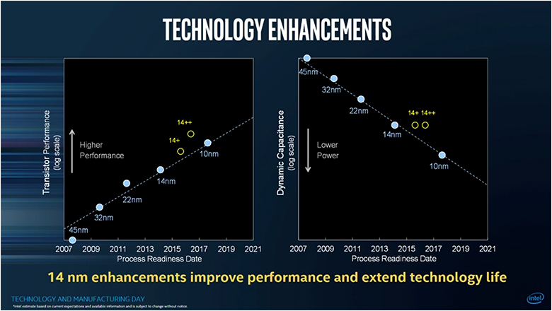
It is also good as this is not the original 10nm fab process. A process that Mark Bohr back in 2017 as being inferior to the 14nm++ node process (https://vimeo.com/intelpr/review/210691247/77b64a2bcd)… and is a big reason Crimson Canyon NUC’s underperformed as badly as they did. It is also not the “10nm+” that made it to market(ish) via Tiger Lake BGA CPUs. Instead, Alder Lake usess a third generation 10nm fab process. An enhanced process which promises another 10-15% gain over the second gen / ‘10nm SuperFin’ node process.
Using a smaller node process is also good as it allows Intel to fit more transistors into each square millimeter of silicon. Think 100’ish MTr/mm² (mega-transistor per squared millimeter) vs 37.5 MTr/mm². This combination, in conjunction with a slightly large socket size (more on this in a moment), is how Intel can fit more cores inside their 12th Generation Core-I series vs. the previous generations of CPUs.
It however does not mean one should expect an average 20 percent or better performance improvement. Instead, this freeing up of power has been used for more… well… everything. More cores. More onboard L3 cache. Better IMC. Basically more. Of everything. Without an increase in overall max power consumption.
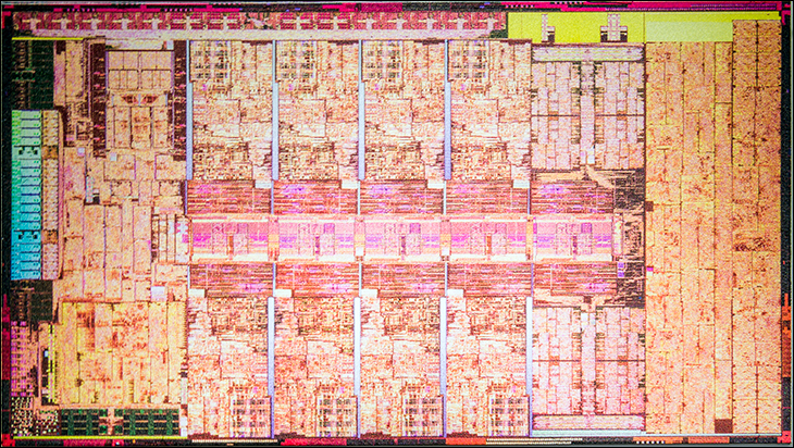
Before we go over that however, there is one thing we have to make clear: There Is No Such Thing As A Free Lunch. When you put more transistors into the same amount of space and feed them the same total amount of power as before(ish)… heat is an issue. Intel is well aware of this and have taken multiple steps to curb heat production and handle said heat when it is created.
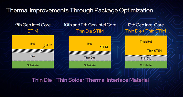
The first step is physical. Modern CPUs are flip chips with the ‘bottom’ silicon substrate layer being ‘on top’ and the transistors below them. A lower z-height in this substrate (aka thinner substrate) means that the heat from the cores has less heat insulating bulk to travel through before it reaches the IHS. In the 10th they started shaving some of this substrate and making the copper IHS (and used solder TIM) thicker, then they thinned it again for the 11th gen… and now its even thinner. Think under 0.5mm tall. Then to further improve heat transfer to the IHS, Intel also made the Solder Thermal Interface Material (aka STIM or sTIM) thinner. Interestingly enough, Intel did not specify a lower Z-height for their new socket 1700 specification. Instead, they kept it the same as Socket 1200. This means more copper in the IHS which in turn means the Integrated Heat Spreader is even better at its job than its predecessors.
Of course, it has to be as the ‘hot spots’ are not smack dab in the middle of the socket. They are offset either slightly above or slightly below the center line (depending on which cores are active and what s1700 CPU you are using). When pushing their Maximum Turbo Power limits they can get toasty… and when manually overclocking them even further they get down right hot. Needless to say, you are going to want a good cooing solution (preferably water based) capable of handling over 250 watts of heat if using the Core i9 and over 150 if the Core i5. Though to be fair that is a downgrade for the Core i5 (the last gen was a fireball that also needed a cooler capable of handling 250+ watts of heat), and pretty much par for the course for the i9 when compared to the 10th or 11th gen Core-i9s.
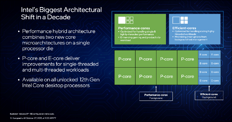
The next way Intel is combating heat is simple: make less of it whenever possible. By taking a page from ARM processor designs Intel’ latest mainstream CPUs no longer consist of all the same core types. Instead, they are broken down into two separate and distinct types: efficient ‘e-core’ cores, and performance oriented ‘p-cores’ cores. The P-cores are basically what was supposed to be the ‘tock’ to the 11th generations 10nm design, and the e-cores are actually next gen ‘Atom’ cores.
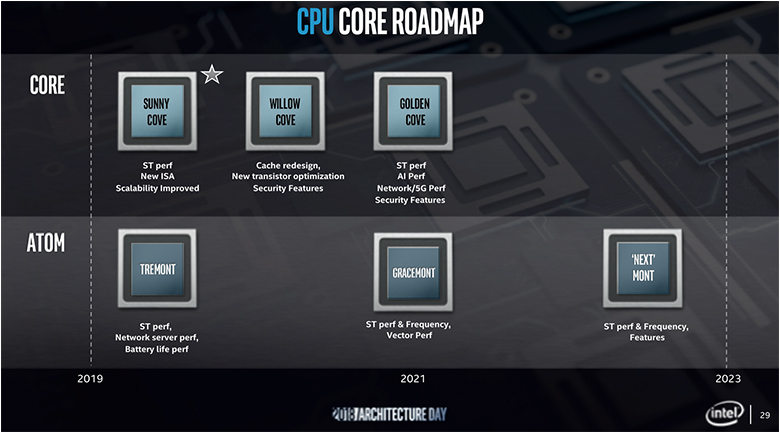
Of the two core types in this hybrid architecture the “Gracemont” Atom cores are the most intriguing. This is not because of rumors of Intel using ‘ARM’ cores… as they are not ARM based cores. They are x64 cores. Instead, their inclusion is intriguing for the simple fact that the Atom CPU design philosophy is one of efficiency above all else… including computational power. That is a radically different philosophy than previous gen desktop CPUs. Basically, Atom CPUs are meant for ultra-low to low powered devices such as Network Attached Storage devices, routers, portable devices, and ‘System On a Chip” type devices where TDP (or “Processor Base Power” in latest Intel speak) requirements are for 10(ish) watts or less. Devices which typically run ARM SoC’s that Intel want manufacturers to convert over to Intel SoCs. Put bluntly Atom design is the antithesis of what desktop CPU’s are all about.
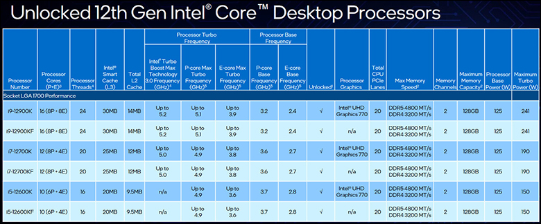
To be fair, these are not typical Atom cores. They replace the ‘Tremont’ design used in Intel’s actual first hybrid CPU design / trial run – ‘Lakefield’. As such they don’t have a 10watt Processor Base Power limit like those found in inside upcoming Android tablets or phones or etc. etc. Instead, their Processor Base Power is part and parcel of the entire Alder Lake Die package. Therefore, even though they may have a base frequency of 2.4GHz (12900k) or even 2.8GHz (12600K) those numbers don’t really mean anything. Sure, they will idle along at that (or lower) if they do not need more power to complete the task they have been assigned… but they can (and will) boost up to 3.2GHz (12900K) or even 3.7GHz (12600K). Equally important is these Atom cores are overclockable. Intel’s own XTU application can/will ‘one click’ overclock them along with the p-cores.
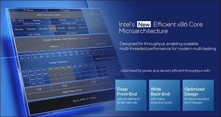
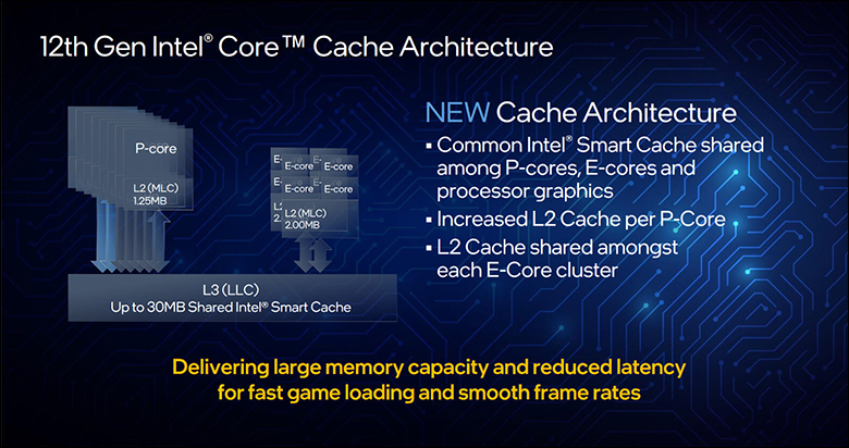
That is just the surface specifications as once you dig into them you realize that Intel has hot rodded them over previous Atom designs. Most blatant of all changes is Gracemont is the first to support AVX2 and even AVX-VNNI (Vector Neural Network Instructions for AVX). It even has 17 execution ports instead of the 12 in previous designs (though we doubt it is physically able to do 17 instructions concurrently). Beyond that however, Intel has bumped up the buffer size and buffed its capabilities. For instance, the reorder buffer size is now a whopping 256; instead of 64KB (32KB data + 32KB instruction) per core of L1 cache each of these have 96KB (64KB instruction + 32KB data) L1 Cache. Each 4-core block / module also has access to a shared 2MB of L2 cache… and most importantly of all the e-cores share the same 30MB L3 cache pool as the p-cores.
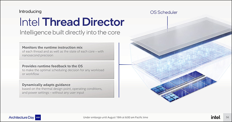
This last detail is critically important as there is a microcontroller baked into Alder Lake. Called Intel Thread Director (ITD… not to be confused with IDT10T), this tiny little microcontroller has a complete overview of what is occurring inside the Alder Lake CPU right down to what instructions are running on what core, what are idle, what new requests are coming in. All in nanosecond time slices. It then, if allowed by the OS’ thread scheduler which it communicates in millisecond time reports, can nearly seamlessly switch the high-level thread from a P-core to an E-core – and vice versa. Thus the easiest way to ‘get’ what it does it to think of it as the ‘supervisor’ for the entire processor. A supervisor baked right into the silicon so as to reduce latency and increase overall performance.

How it chooses where each thread should start out and where it should end up is elegantly simple, yet rather complex in its logic. The first 6 (12600K) or 8 (12900k) threads to come online are immediately shunted to the 6 or 8 p-cores. One thread per core to be precise. When a new thread becomes active the ITD checks to see if it is a high demand or low demand thread. If low it shunts it over to an e-core. If it is suspected of being a high demand thread it swaps out a lower resource / power intensive thread active in a p-core to an e-core. Then it puts the new active thread in a p-core. When all the p and e-cores are actively working on threads and another thread becomes active it either shunts it into a HyperThreading state on the ‘best’ p-core or moves an e-core thread to this HT spot and places the new thread in an e-core (which ever will save the most power while still meeting processor demands). After all HyperThreads are active… things get complicated with resources having to be shared and threads juggled from e to p cores on a case by case basis. Once again. Simple(’ish) to describe but with a ton of highly complex logic and rules required to make it work in real-time.

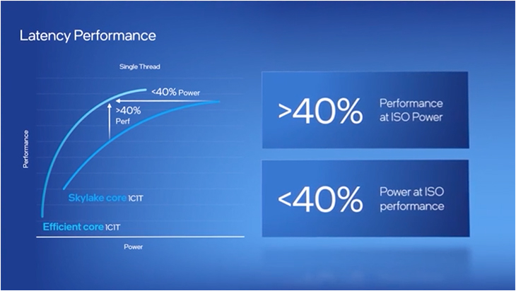
Since the e-cores are optimized to sip as little power as possible (a little more than half of a Skylake core) and taking up as little room as possible (a 4 e-core block is about the size of one 1 p-core), while also providing a lot of power (claims put it at about 8 percent higher performance clock for clock than Skylake… and yes we are drooling at the idea of a next gen 72 or 80 core ‘HEDT’ made up entirely of e-cores) they are not HyperThread enabled. That is why the Core i5-12600K is classified as a 10 core, 16 thread CPU while the Core i9 is a 16 core, 24 thread CPU.
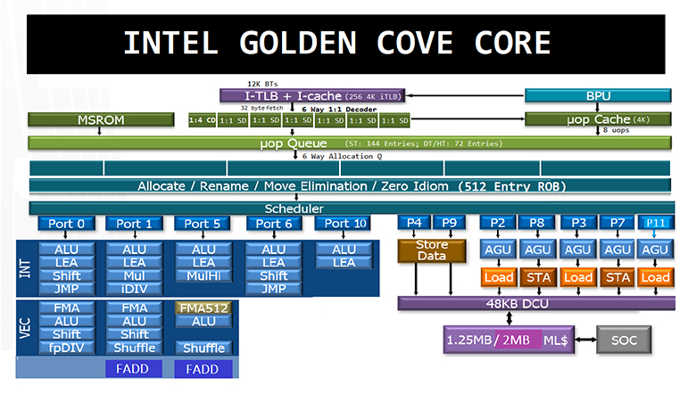
That nicely segues into the P-cores. The ‘Golden Cove’ microarchitecture is rather advanced and has a lot of buffed features versus the backported Cypress Cove design it replaces. First and foremost is this team did not have to worry about trying to fit the end result into a socket 1200 (square 37.5 x 37.5mm) form-factor. Instead, it uses the new (rectangular 37.5 x 45mm) socket 1700.
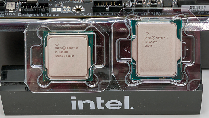
This is a good, an ironic, and a not so good thing. All at the same time. It is good as more room means more pins (thus the ‘1700’ in the name). It is ironic as it is possible that Intel was not sure they would get their ‘7’ process up to snuff in time… as the new dies only take up a bit over 215 square millimeters vs. the 11th gen’s 276 square millimeters.

The not so good, is that unless the motherboard offers reverse compatibility baked into the PCB (e.g. some Asus come with mounting holes for both s1200 and s1700 around the socket)… your existing CPU cooling solution and most likely those on store shelves right now will not work. Noctua, CM, Scythe… basically every cooler manufacture is offering free s1700 mounting brackets. They will however take time to get to you after you purchase a cooler. Thankfully some forward thinking manufacturers like Gigabyte baked s1700 support right into their designs (e.g. GB WaterForce X line comes with s1700 support ‘right out of the box’). So, if you are impatient make sure to purchase a cooler that is already fully compatible with your shiny new system.
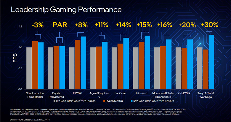
Moving on. Intel has made a big deal about IPC and wanting to regain the crown AMD and their Zen 3 snatched from them recently. Intel claim that Alder Lake offers 19 percent IPC improvements over their 11th gen… and after testing they are correct. With an asterisk and an ish. The asterisk being that there is only 8 p-cores that are blazing fast in this ’16 core’ i9 and only 6 in their ’10 core’ i5. IPC is all well and fine as long as you understand that only 6-8 threads are going to be blazingly fast because of it. This is why gaming performance is going to be somewhat variable – to the point even Intel claims a -3 to 30 percent boost over previous gen 11 CPUs. In testing… yeah even the piddly little i5 can routinely produce gobsmackingly better performance than any i5 has the right to have. Think sometimes even better than last gen i9. Put bluntly, in most games, if you want the best frames per second that money can buy you want a 12th Gen Core-I processor.
The ‘ish’ comes into play in that the new Gracemont cores may be incredibly fast for ATOM cores… but performance does drop off as more and more in a given block are loaded. Basically, when only 1 of a 4 e-core block are active they have plenty of cache and thermal headroom to handle the task. Handle it so well you would almost think they were a couple generation old Intel CPU core(s) and not freakin’ Atom cores. However, when all four are active performance does suffer. There is still not enough cache to keep it from having to go out to L3. Also, Intel is being rather aggressive in keeping their Processor Base Power (and thus power consumption) as low as possible. Overclocking can indeed help… but they do get toasty rather fast once pushed above their stock Turbo settings. That is one mean one-two combination when it comes to performance consistency.
Basically, if one is active you can almost consider it the same as a similarly clocked 7th or 8th gen Intel core, but all are active? Then its ATOM roots start showing and showing badly. Of course, this only holds true when either all e-cores are on high demand threads, or you are using a ‘core aware’ application that can crush 16…32… even 64 core processors. When dealing with 3 or sometimes even 2 low demand threads and only 1 (or sometimes 2) high demand on a 4 e-core block… that e-core block is rather peppy and you will probably not know for sure if a thread is on an e-core or a p-core. That is rather impressive, but still something to consider when comparing Intel to AMD for your next upgrade.
Honestly, this variability is a good argument in the Core i9’s favor as you can have ten active cores without really knowing you are using a ‘hybrid’ CPU design. Ten cores is a lot of active, high demand threads. Of course, the Core i7-12700K offers 8 p-cores and 4-ecores for $180 (USD) less than the Core i9. Only you can decide if nearly 2 bills for one extra high(ish) performance(ish) thread is worth the entry fee or not. Our opinion is that it is worth it… as this is the first mainstream Intel CPU that outperforms their 10th gen core i9-10900K beast.

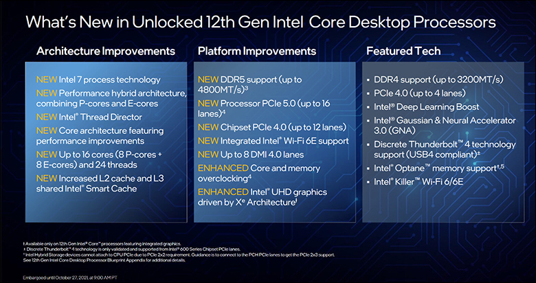
Moving on and circling back to the list of changes. We have already gone over how Intel is helping to control heat via different methods (thin, hybrid, footprint). The biggest, for us, is two-fold. The first is DDR5 capabilities with DDR4 backwards compatibility baked right into the Integrated dual-channel Memory Controller. To be specific, DDR4-3200 and DDR5-4800 are the max ‘native’ memory frequencies supported right now. The obvious caveat is… its an either/or deal. You either use a motherboard with DDR4 DIMMS or a motherboard with DDR5. No mix and matching allowed.
The other caveat is… you really will want to go faster than DDR5-4800 if you want Alder Lake to really stretch its legs. Its IMC is first gen tech, and it occasionally does throw a wobbly with latency spiking well above the theoretical 16.67ns that DDR5-4800 ‘should’ be. These spikes virtually eliminate any performance benefits DDR5 brings to the table unless you go as fast as you can as long as you can. To the point that we would “overclock the IMC” by using even faster DDR5 RAM… and going as high as the RAM would allow us. Considering even mundane DDR5 is expensive, that is not a cheap endeavor. Though to be fair, this could only be a short-term issue and a simple micro-code update could fix it (or at least mitigate it). Such updates have happened in the past and probably will in the future (just think of all the AMD ‘AGESA’ updates AMD has released in the past couple years that are RAM related). After all, these days it seems all PC components are released in their beta stage and it takes a good 6+ months before they really become ‘fully baked’.
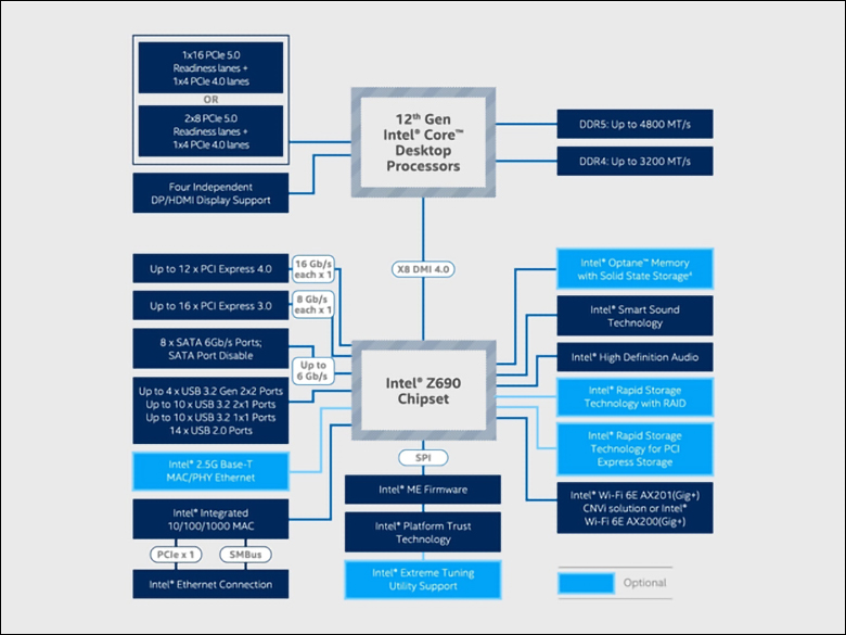
The other big improvement is both highly exciting and yet highly frustrating at the same time. We are of course referring to PCIe 5.0… of which there is a grand total of zero PC components available right now. Maybe mid to late next year we will see GPUs and maybe even NVMe drives (if Phison is to be believed) take advantage of this massive bus, but it is a ‘future proofing’ type feature. Also, Intel has not increased the number of lanes powered by the CPU. It still is 20. In fact… its 16 PCIe 5.0 + 4 PCIe 4.0 lanes… with the four lanes meant to be used by the motherboard manufacture for a M.2 drive. In other words, if PCIe 5.0 NVMe drives start appearing not every motherboard’s M.2 slot will be able to run them. In many instances owners will have to purchase M.2 to PCIe board adapters and split their 16 PCIe 5.0 ‘GPU’ lanes into two x8s – thus nullifying PCIe 5.0 x16’s bandwidth advantage over PCIe 4.0 x16.
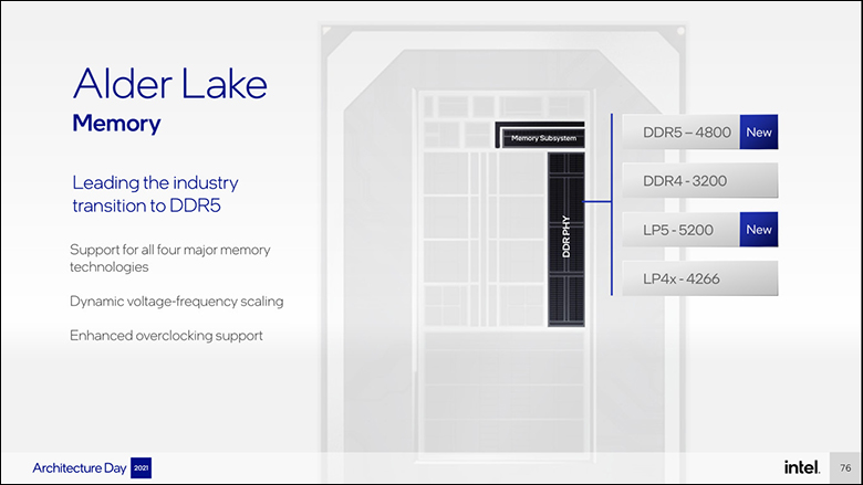
On the positive side, in order to handle DDR5 and PCIe 5.0 bandwidth requirements Intel has beefed up the internal interconnect bus(es). The Compute Fabric (what allows all the blocks of e and p cores to communicate with each other and their cache) is a whopping 1000GB/s (or one frickin’ TeraByte of data per second). The Memory fabric portion of the internal interconnect is now rated for 204GB/s… or basically the same as what Intel uses in their 8-channel Ice Lake servers CPUs. Also beefed up is the CPU to chipset bus which is now 64GB/s… aka PCIe 5.0 x16. That is a lot of uber wide buses that should help the spice… err… data flow… and flow it must.
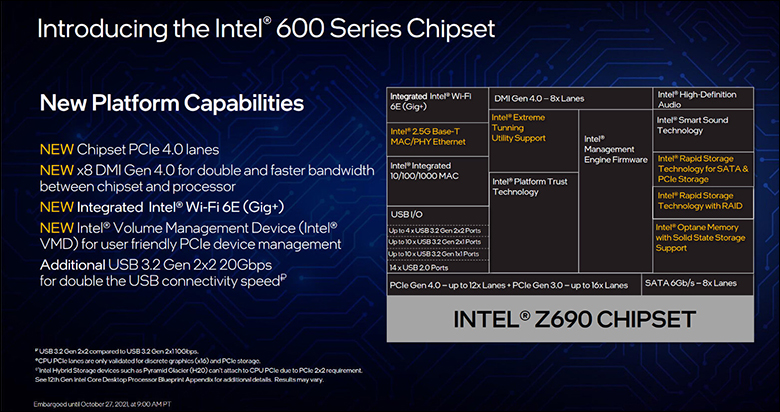
Not to be outdone the (14nm fabed) Z690 chipset has also been boosted in the bus bandwidth departments. Simply put everything has been upgraded. Z690 offers 12 PCIe 4.0 lanes and 16 PCIe 3.0 lanes all by its self. The all important DMI link is now “DMI 4.0” and as the name suggests it is PCIe 4.0 x8 capable (or twice the bandwidth of Z590’s DMI 3.0). Of course, it had to be upgraded as it now supports a veritable cornucopia of high bandwidth devices. Native support for eight SATA drives, (up to) 4 USB 3.2 Gen 2×2 ports (aka USB 20Gb/s), 10 USB 3.2 Gen 2×1 (10Gb/s aka USB 3.1 gen 2 / og USB 3.1), and ten USB 3.2 Gen 1×1 ports (5Gb/s… aka USB 3.0).
Further upping the ante, is thanks to Intel splitting it into PCIe 4 and PCIe 3 lanes, motherboards can save the high bandwidth bus for things that need it. Say stick dedicated mouse or keyboard ports on the 3.0’s and then use the bigger bus for demanding peripherals like say USB 4.0 (when it lands), or Thunderbolt 4, or even Wi-Fi 6 (that is now baked into Z690). Put bluntly, Intel is giving motherboard manufacturers a lot of freedom in how they split the lanes and thus allowing it to live up to its name of ‘Flexible High Speed I/O’.
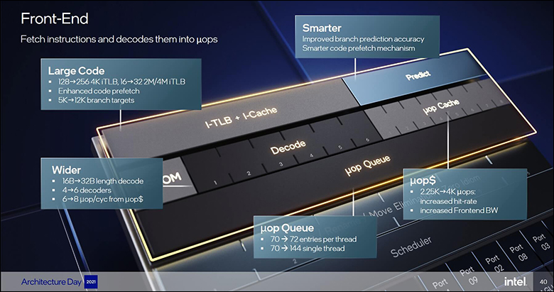
Circling back to the p-core architecture… and boy a lot has changed. While AMD was saying that going beyond a 4-wide instruction decode strategy would result in potentially worse performance… Intel went ahead and did a 6-way. Then doubled the fetch bandwidth to 32bytes per cycle to help feed that hungry beast. Though to be fair, Intel is well, well aware of AMD’s point. That point being that if the decoder gets it wrong… it is a massive (double digit) penalty in lost processor cycles.
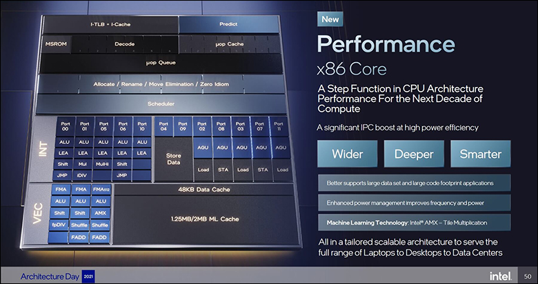
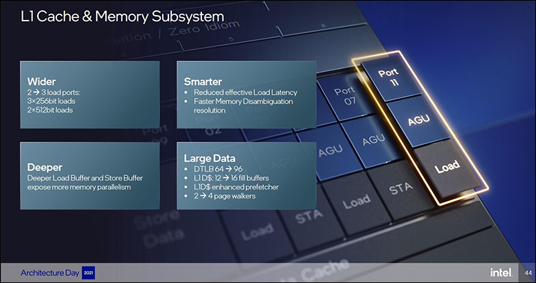
To help ensure that this does not happen all that often, Intel has done their best to make sure that the core did not have to rely on a costly decode operation at all. To this end they also went ahead and nearly doubled the micro-operation (‘μop’) cache from an already large 2,250 entries in the 11th gen to 4,000 entries. Then basically increased its bandwidth to 8 from 6. Then doubled the L1 instruction cache entries from 128 to 256. Then increased the L1 data fill buffers from 12 to 16.
Since someone was already holding their beer… they even increased the L2 Branch target buffer from an already large 5,000 entries to a whopping 12,000 entries. Improved the pre-fetchers via a “full-line-write predictive bandwidth optimization” strategy (aka fuzzy math that makes even most genius head hurt when they try and think about it). Then to just add salt to the wound they increased the re-order buffer from 352 to 512 entries to improve out-of-order instruction performance. About the only thing that is not massively improved is the execution width of 12 (up from 10)… which is lower than the e-core’s 17. The same is somewhat true of the L3 cache. On the one hand the i9 now has 30MB (up from 20MB) and the i5 has 20MB (up from 12MB)… but it is spread out over more ‘cores’. Basically, instead of 2MB per core it is now 1.875MB for the i9 and 1.66MB for the i5 (ironically enough the i7 and its 25MB of L3 cache is actually more per core at 2.1MB).
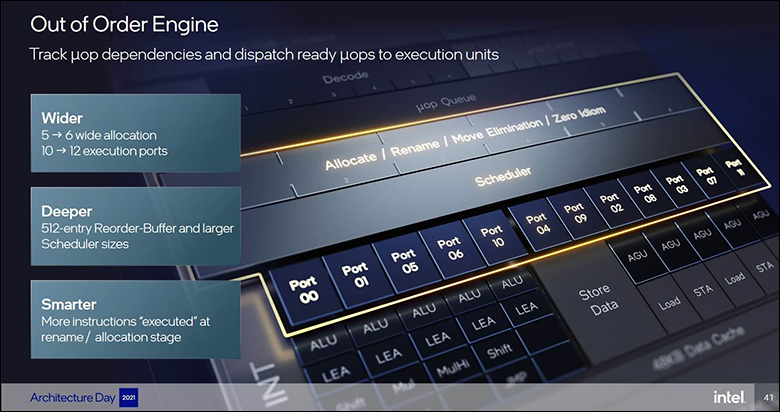
Needless to say, that is a lot of low-level improvements. A lot of low-level improvements that take a lot of time and effort to get right. When they do get it right, as they obviously did here based on test results… it all but guarantees higher IPC in the real-world. Intel states it is an average of 19 percent improvement over last gen, and in many cases they are actually being rather conservative. Of course, in other cases they are being… overly optimistic.
To be fair, IPC has not been Intel’s sole focus as performance per watt was just as important. They also wanted to improve multi-threaded performance… as the software world is slowly becoming more and more multi-threaded. Splitting their focus means less improvements in any on area but better overall improvements. The most obvious multi-thread improvement is the Memory-level parallelism (MLP) capabilities. Here they have been improved with Golden Cove being able to handle 48 outstanding requests from 32 in the 11th generation. Once again, something that takes a lot of time and effort to implement… but when implemented properly boosts overall multi-thread performance higher than ever before.
Zooming out to the big picture some things have changed and some have remained the same. For instance, the iGPU is firmly in the not much has changed category. Sure, it has DirectX12 support, but it is more a refinement of the previous UHD 750 found in the 11th gen rather than offer the massive gains the 750 had over its predecessor. Though to be fair, it will be slightly faster and offer slightly higher FPS via a small frequency boost of 250 Mhz over the UHD 750’s 1300(i9) or 1200(i5). with the i9 ironically getting the better boost clock of 1550Mhz vs 14450 for the i5.
Interestingly enough, both the Core i9-12900K and the Core i5-12600 basically have the same frequency settings as their 11th gen predecessors. In the Core i9’s case that means 5.3Ghz (1-2 cores only) via Thermal Velocity Boost, and 4.9Ghz for the Core i5. The Maximum Turbo Power (aka “PL2”) of the core i9 is basically the same at 241 with a similar Tau setting. However, the Core i5’s Maximum Turbo Power has changed. A lot of buyers of 11th gen i5’s did not realize they were set to volcano mode at the factory like the Core i9s and complained… so Intel toned things down back to essentially 10th gen days. Thus, instead of 251 watt the Core i5-12600K has a 150 watt setting. Of course, manufactures can ignore it as they are more… guidelines than rules – just like it was in the 11th gen days.
L1 and L2 cache changes really cannot be directly compared to the 11th gen. The ‘Gracemont’ Atom cores are designed to be cache heavy to boost performance up to reasonable standards. Thus, the e-cores come with 16KB per core more L1 than the Golden Coves (64 instruction + 32 data vs 32 instruction + 48 data) and 0.75MB more per core L2 cache (2MB vs 1.25MB). Either way, Intel is relying on a lot of cache to help boost performance… as (up to) 1408KB L1 and (up to) 14MB of L2 is an insane amount of low level cache for a mere mainstream CPU to have access to. Heck, that is almost as much as what the 11th Gen Core i9’s L3 cache was (16MB)!

Surprisingly, the last major thing that has and has not changed is overclocking. DDR4 vs DDR5… meh. A bit different when it comes to voltages (as DDR5 is 1.1v instead of 1.2v) and frequencies (way higher)… and CAS latency (way… way higher), but if you have overclocked DDR4 you pretty much can overclock DDR5. Just keep the voltages in check and do things like you would on your DDR4 rigs. We say this as even though 12th Gen’ers have Dynamic Memory Control baked into the IMC only time will tell if it is something worth using… as latency is already an issue with DDR5 and Intel 12th gen CPUs.

CPU overclocking on the other hand? Instead of having to tune (and worry about) one type of core you now have two separate and distinct core architectures to deal with. Thankfully they are considered distinct by Intel’s XTU program and thus can be dialed in one type at a time… albeit with e-cores it is more precise to say one block at a time as you can not dial down to individual e-cores; whereas as with p-core you can dial in each core individually if you so choose.
With all that said, it quickly became apparent that while you can overclock the e-cores… they rapidly become temperamental and start generating heat. Heat in larger quantities than their small form-factor and name would lead one to believe is even possible. So much so that you will want good cooling if you plan on going down the manual overclocking road. This is true for the both the Core-i9 and Core-i5… but of the two the Core-i9’s e-cores go from warm to thermal limiting much… much faster. This is not all that surprising as there are twice the number of them being shake n baked by increased voltage (and frequencies). As such we suggest keeping the e-cores in the low (i9) to mid (i5) 4Ghz range if you want to ensure long term stability. This is a shame as their behavior when heavily stressed does become noticeably peppier the higher they are pushed.
Thankfully, the p-cores are pretty much the ‘same old same old’ when it comes to Intel Core-I overclocking. In fact, they are rather predictable. Maybe even more predictable than the last generation. So, if you really do not want to go down the dual overclocking road the p-core sandbox is where most novices will want to play. Hitting 5.3 to 5.5Ghz (i5 / i9) ‘all (p-)core’ frequencies should not be all that onerous an endeavor if you are doing p-core only overclocking. However, we prefer a much more balanced, and long term stable, approach to overclocking. Thus we applied only a moderate overclock to both e and p cores. In the case of i9 a 5.3 p and 4.2 e “all” core overclock, with the i5 at 5.0 p and 4.3 e ‘all’ core overclock. Just be warned. This will suck down power basically as badly as the past generation… and pump out heat like nobody’s business. Just like the last generation. Thus, good cooling is, once again, a de-facto requirement if you want the best performance possible from your new Intel CPU.
Overall, we are highly impressed with Intel’s Alder Lake team has been able to accomplish in such a short time span. Impressed enough that the fact it is being built on a 10nm node process is the least of it. Now let’s see what they can actually do and see if this whole ‘hybrid’ idea makes sense.
