As the A10-7890K is an APU design the best place to start is by describing exactly what an APU is. An APU is an Accelerated Processing Unit and basically is a CPU (Central Processing Unit) with an GPU (Graphics Processing Unit) built right on to the same piece of silicon (aka ‘on-die GPU’). However, this does necessarily mean a larger number of pins are required. To be precise AMD’s FM+ APU’s use a 906 pin design (with the pins being on the APU and not the motherboard’s socket) instead of 941 pins AMD’s AM3 processors require.
How is this possible? Simple. Good engineering… and a lot of time, effort and experience with doing a true dual purpose processor. To be precise Godavari is a fifth generation design and is the second generation of AMD APU’s that uses a Heterogeneous System Architecture (HSA). As we saw in the A10-7800 review, HSA does make a difference and does allow core components that date back to early 2014 to compete with Intel 2016 designs… and win on the video front andoverall value front – while doing a darn decent job on the CPU front as well.
When Godavari was announced many assumed this second generation HSA APU would be a radical change from Kavari. That is not the case. Instead Godavari is heavily based on Kaveri. In fact, beyond some minor low level tweaking to the architecture that increases efficiency, Godavari is a Kaveri… on steroids. Basically AMD focused on making the best Kaveri design possible on a 28nm fab process and then moved on to the upcoming ‘Zen’ architecture that will be new and potentially radically different.
On the surface this does sound disappointing, to say the least, but the fact of the matter is Intel does the exact same thing with their ‘tick-tock…tock’ cycle. Put another way, besides the missing node shrink AMD are doing exactly what Intel has done for many, many generations. For those who really, really want a brand new architecture October should be an interesting month (as ‘Zen’ is alleged to be landing). In the meantime, Godavari has a lot of horsepower under the hood and is still one potent all in one processor.
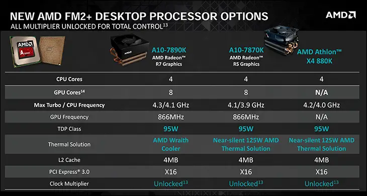
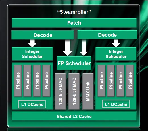
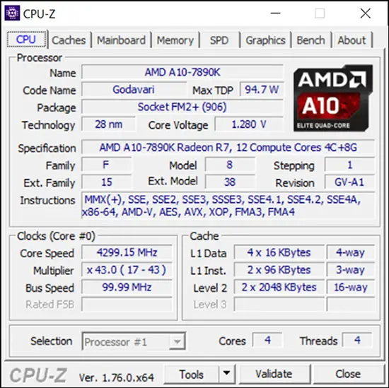
So what is a Kaveri 2.0… err Godavari APU made up of? Basically it is the same as a A10-7800 (or if you want to pedantic a A10-7850K) but at higher clock rates. This means two CPU blocks for a total of four Steamroller based Compute Units running at a maximum speed of 4.3Ghz (up from 3.9Ghz in the fourth generation A10-7800).
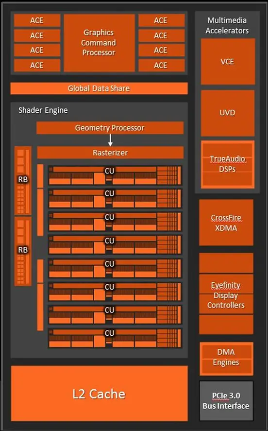
For the ‘GPU’ portion of the core the A10-7890K has eight video Compute Units… just as with the previous Kaveri. However, while it is indeed true these eight graphic Compute Units are based on an R9 2-series design, they are now running at 866Mhz (up from 720Mhz) and still boast 512 stream processors, 128 Texture Units and all the other sundries that make up a modern AMD 2-series R-7 ‘GPU’.
Also as expected to make all twelve of these Compute Units work together as one cohesive whole AMD’s HSA layer resides ‘on top’ of them. This in turn means the four CPU Compute Units can create and send work directly to the eight video CU’s and vice versa (via what AMD calls heterogeneous Queuing, and the industry simply calls Dynamic Parallelism). Better still this cross flow of GPU calling on CPU functions (and vice versa) is all done at the kernel level and does not require OS, API, or even drivers to do so. Instead it is bare-metal crosstalk that is a lot more efficient than a discrete CPU and GPU… or even an older APU’s ways of doing things.
More importantly is the twelve cores now share the entire RAM amount as one large memory unit instead of dividing it upon POST into two parts… that could not be shared or even ‘seen’ by the other Compute Unit type. This is called hUMA (heterogeneous Uniform Memory Access) and works darn good and requires a lot less TLC than the old way of dividing and hoping one type does not run out of memory. The works loads are also now equally spread across all the CUs and each CU knows what the others are working on so as to not cause issues with writing to memory sector that another is reading (‘Platform Atomics’).
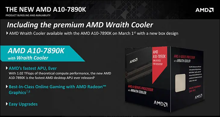
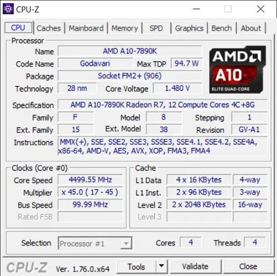
Basically the A10-7890K is a super-clocked A10-7800 (well really a A10-7850K) but at a higher TDP (now 95 instead of 65). Also noteworthy is the additional $40 ‘surcharge’ that the ‘7890K demands over the older ‘7800 is it is a ‘black’ processor. In layman’s terms this means it is an unlocked processor that allows for rather easy overclocking of both the ‘CPU’ portion and the ‘GPU’ portion. In testing we easily pushed the four CPU cores to 4.5Ghz and pushed the GPU cores to 1040Mhz. That is damn impressive considering we did all that and still did not hit the 72-degree thermal wall. Needless to say AMD’s Wrath stock cooler is one beastly cooler that allows consumers the luxury of spending money on other things… without really limiting overclocking. Color us impressed.


