Zen 2 hitting Intel where it hurts – the mainstream market
It is hard to imagine but it has now been more than two years since AMD rocked the CPU industry with the release of their “Zen 1.0” based Ryzen 1000 series. In the interim, AMD did release a minor refresh in the form of the ‘Zen+” Ryzen 2000 series (dubbed by many as Zen 1.5) that brought a fabrication nod size reduction (12nm instead of 14nm), as well as some under the hood modifications to make the Zen processor design more efficient. The Ryzen 2000 was indeed a nice, and much needed, upgrade to AMD’s lineup. However even the Ryzen 2000 models were intended to simply bring CPU performance parity back to the marketplace and allow AMD to compete against Intel in more than just the ‘value’ end of the marketplace. Mostly it did this by being both less expensive and offering more cores than Intel’s mainstream / non-HEDT processor options.
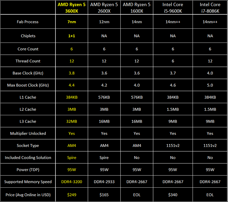
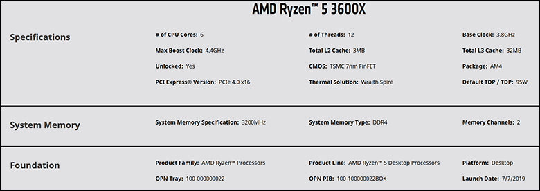
Recently AMD released the all new Zen 2 based Ryzen 3000 series and this time has a rather ambitious goal in mind: market dominance. Today we will be focusing in on the more typical ‘every man’ option of their new Ryzen lineup. The Ryzen 3600X, which offers 6 cores / 12 Threads, running at 3.8 to 4.4GHz, and yet only has an MSRP of $249 US. This processor certainly is not a Ryzen 3000-series with the highest core count (Ryzen R9 3950X with 16 cores and 32 threads), the fastest Ryzen 3000 CPU (also the 3950X with single core boost rating of 4.7Ghz), nor even the least expensive (Ryzen 3 1200 with an MSRP of $109 USD). Instead the 5 3600X sits right in the middle of the lineup with a relatively low asking price and yet high (enough) core count. This is generally the sweet spot most people call ‘value’, and its overall value is meant to take buyers away from Intel’s largest consumer CPU market: you the average buyer who use a system for everything from ‘gaming’ to ‘work’ related tasks.
AMD intends to do this by not only capitalizing on Intel’s ongoing fabrication woes, but by making a CPU that is simply more efficient than ever before. Yes, for the first time since the days of AMD’s X2 series, AMD is focused not in on competing against Intel but beating them. Beating them at their own game. Beating them by not concentrating on shear frequency scaling, or number of cores, but on Instructions Per Clock cycle. Strip away all the fancy marketing and if you have two competing products running at the same speed, the one that can offer more IPC’s will be the ‘faster’ processor. This is especially true of PC games and other single, or low, thread count applications.
Ryzen 1.0 and Ryzen 2.0 did indeed make great strides to get to parity, but there was still the equivalent of a couple hundred MHz handicap on Zen 1 and Zen 1+ designs compared to Intel’s latest and greatest. Thanks to Intel and their lackluster IPC improvements in the past couple generations, AMD saw this as an opportunity and thus Zen 2 was born. We will go over not only how they obtained IPC improvements, upwards of 15 percent, but also how these improvements translate to real-world benefits. Specifically, how they compare to AMD’s last Ryzen 5 series and Intel 8 and 9 series. If Zen 2 can indeed deliver on its promises, the AMD Ryzen 5 3600X may just become the default processor to buy for large swaths of the buying public. A processor that offers excellent single threaded performance, enough horsepower for heavily threaded applications and yet only set buyers back less than $250…. which on paper certainly sounds like an excellent way to redefine value.
Features and Specifications

Overview of Zen 2 (Physical Differences)

Let us be perfectly clear. AMD’s Zen 1 / Ryzen 1000-series was a paradigm shift for how CPUs were created. By moving away from ‘monolithic’ CPU design to a building block design the ramifications of this innovation are still be felt today in the industry. So much so Intel hired ex-AMD employees to help create their own take on ‘Lego block’ design.
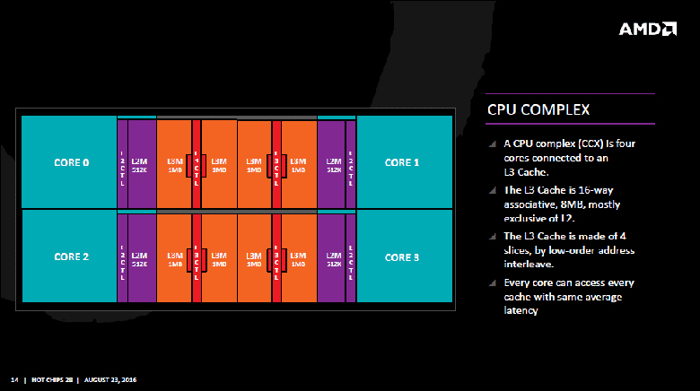
As a brief overview, Zen 1 architecture was based around the idea of Core Complex (CCX) ‘blocks’. These blocks contained four ‘cores’ (with anywhere from 0 to 2 of them deactivated), the memory controller, the IO controller, various L1-L3 cache, etc. The more CCXs you add to a ‘CPU’ the more powerful the end result is. This is why many refer to them as ‘Lego Blocks’. Of course, as these CCX blocks need to communicate not only with the rest of the system (e.g. the RAM or PCIe bus, etc. etc.) but also with other CCX’s AMD upgraded/revised their HyperTransport Interconnect technology to handle this increase in load. The end result is the Infinity Fabric that consists of two separate communication planes: Scalable Data Fabric (SDF) and Scalable Control Fabric (SCF). As the name suggests SDF portion of Infinity Fabric handles communications with the rest of your system, whereas SCF handles inter-CCX communications.
This combination was ingenious as it allowed AMD to easily scale up or down an entire product line-up, use more of the fabrication wafer (as a ‘bad’ CCX could be usually salvaged for lower Ryzen / ThreadRipper ‘CPUs”), and even easily create models with integrated graphic (what AMD calls “APUs” and have a ‘G’ at the end of the model). This increased flexibility also allowed AMD the ability to not only create higher core count CPUs than Intel, but be much more agile in reacting to changing market demands.
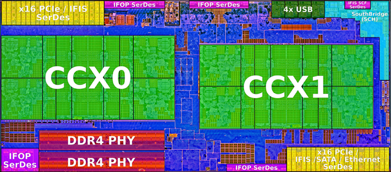
The downside is this design may be modular but is still based upon fully functioning, highly complex CCX’s which required a lot of die space for secondary controller. Each CCX needed everything from integrated memory controllers on down and are basically miniature “monolithic” Central Processing Units… just ones created and used in a radically different manner.
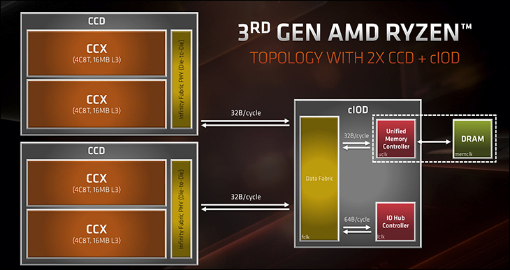
This is how Zen and Zen+ processors were all designed. Zen 2 / Ryzen 3000-series does things drastically different. Instead of designing CCX ‘blocks’ that do everything, AMD has split the processor design into two separate and distinct portions – or in more technical terms a “multi-chip module” (MCM) design.
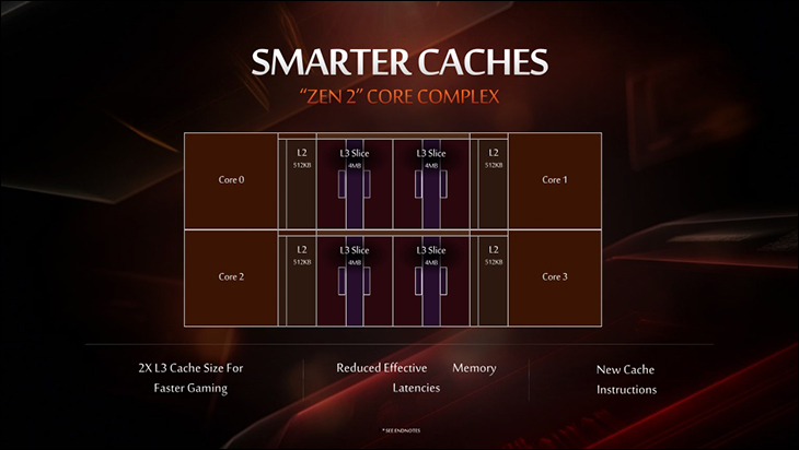
The first is a ‘chiplet’, called a “Chiplet Core Die” (sometimes referred to as a “Client Compute Die”) or ‘CCD’ for short. A CCD houses two noticeably less complex CCX groups of four processing cores (of which an entire CCX or even just cores in a CCX can be disabled). These new CCXs only contain the cores, L1/L2/L3 cache, and Infinity Fabric 2 pathways to connect the cores to the other new chiplet introduced with Zen 2. No memory controller. No inter-CCX communication pathways. Nothing else beyond what is needed to crunch numbers and talk directly to the other new chiplet.
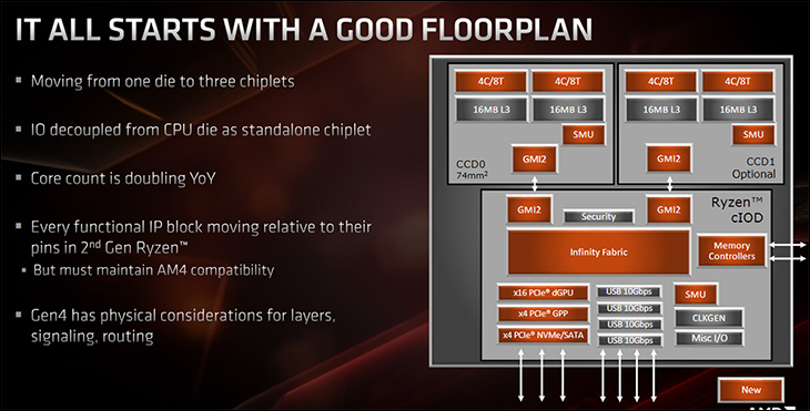
The second portion is an aptly named chiplet I/O Die – or ‘cIOD’ for short. This separate die on the MCM package (or “CPU”) is the central processing hub responsible for all the various portions which used to be housed inside the CCX. Including the SDF and SCF “Infinity Fabric 2” controller. In simplistic terms one can consider this IO chiplet as the middle man that handles all the low level I/O grunt work, allowing the CCX cores in the CCD to actually worry about just crunching numbers.
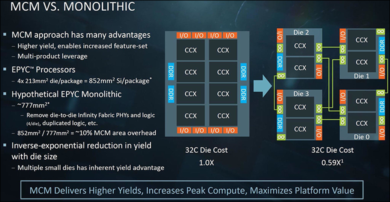
This change does numerous things, but the largest is it allows AMD the luxury of not having to build complex building blocks and then fail complex building blocks just because of a fabrication error in the memory or other secondary controller transistors. Instead they can create more chiplets per wafer and fail fewer of them. Equally important by removing these portions of the ‘classic’ CCX this in turn frees up space for more important things like doubling the L3 cache from 8MB per CCX to 16MB (or 32MB per chiplet… even if the entire chiplet’s cores are not enabled – e.g. 3900X has 64MB with only a chiplet and half worth of CCXs enabled).
This removal of components from the CCX also means that Zen 2 is a Uniform Memory Access (UMA) based system not Non-uniform Memory Access (NUMA) like Zen 1 and Zen+. Questions over NUMA vs UMA for home users is really a non-issue. Both have their positives and negatives. For example, NUMA can result in lowered RAM latency in best case scenarios, but can result in rather high and rather random latency peaks. In the server world, NUMA is a four-letter word for high performance applications which demands consistent low latency results. Work arounds have been done via software to minimize this issue, but UMA does not have it. With UMA all cores access the same memory controllers, resulting in a more consent average latency. Thus Zen 2 in the server market is going to be a very big deal… but for home users it really is not that big a deal.
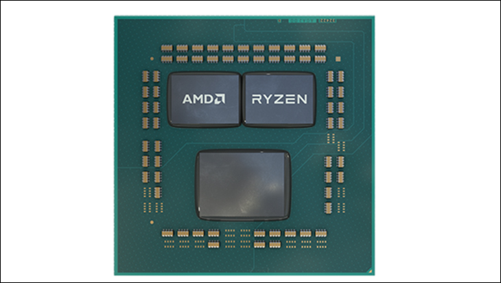
This new multi-chiplet design also allows AMD the luxury of not wasting 7nm fabrication time, or space, on secondary controllers which do not need this expensive fabrication node. Instead, the IO chiplet is being built on 12nm fabrication process. This not only decreases the overall build cost of a Zen 2 based CPU but also allows them to upgrade the IO chiplet’s features without “throwing out” any of the expensive 7nm processing chiplets already fabbed.
The downside, is by offloading the low-level controller to a secondary chiplet, the CCDs can no longer communicate directly with other CCDs. For processors which only house one CCD and one cIOD chiplet this is a moot issue; however, the 12 core Ryzen 9 3900X and Ryzen 9 3950X house two CCD’s. This means inter-chiplet data sharing has to not only cross the Infinity Fabric bus twice but also has be processed through the IO chiplet before reaching the other CCD. This will increase latency, but it is more of an edge case. One which will not happen all that often in-home user scenarios. This is thanks to upgrades in the processor scheduler and predictive math algorithms which were enhanced to take advantage of this new design.
Overview of Zen 2 (Low Level Improvements)

In addition to the innovative physical design changes that Zen 2 brings to the table, there is also numerous low-level improvements. These improvements are how AMD is targeting IPC parity with Intel.
The first and largest improvement has nothing to do with Zen vs Zen 2. Instead it has to do with the fabrication size. By shifting to 7nm node size, AMD claims Instructions Per Clock cycle are increased by a full 15 percent from Zen 1.0 (not Zen+). This is not because they are clocked higher, which does not matter in IPC calculations, rather it is because each component takes up less room. When combined with less complex CCX design, this combination allows more space in the CCD for cache and the inclusion of ‘smarter’ cache designs. It also means more time and room for designing an improved branch prediction unit that is bigger and smarter than its predecessor.
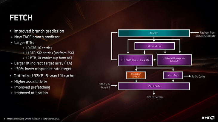
In modern CPUs, an extreme amount of resources is spent on the integrated branch prediction unit. This is part of the “front end” of a processor which not only receive the incoming execution requests but guesses at how set of instructions (or ‘branch’) will go before it actually is complete. How it guesses at future needs involves a lot of math. In simplistic terms if someone says “hand me 1, hand me 2, hand me 3” you are going to assume the next is “4”. Congratulations you just predicted the future of that ‘branch’ of requests using historical data you stored in your ‘cache’. This is basically what branch predication algorithms boil down to: preloading as much as possible so that the core is not wasting cycles idling using recent history of already processed requests. This is sometimes called ‘pre-fetching’. The smarter the predictor unit the higher the IPC the processor is rated for.
Zen 2’s branch prediction unit consists of numerous parts. The first is an all new branch predictor which uses TAGE branch predications. TAGE stands for TAgged GEometric branch predication and uses a hybrid approach to branch predication. What this means is it not only keeps a history of all predications it made but tracks the accuracy of its guesses (‘tagging’ them). Then when it needs to do new branch prediction it looks at the historical predictions it made, picks the one that fits what it is working on, and when multiple records are found… picks the one that it got right more often than the other choices.
To imagine this, let’s build on the example we already used. If someone asks you for 1 then 2 then 3 multiple times a day and you guessed 4 the first time, got it right, but guessed 5 the next time and got it wrong TAGE will tell you to guess ‘4’ the next time that scenario pops up. The down side is TAGE is not precisely fast compared to simpler prediction methods. This is why TAGE is only being used for L2 branch predictions, not L1… and not all L2 predictions. On top of TAGE is the previous generations L2 Branch Target Buffer (BTB), this simpler (but faster) approach is now backstopped by a 7K entry (or history) capacity buffer which may not guess as right as TAGE but with such a large history buffer to look through the loss of processing cycles is minimized. Basically, and overly simplified, TAGE is used for complex and large branches where a little bit of time up front can save a lot of cycles later, and BTB is for shorter and smaller branch predictions where the latency penalty would be greater than a ‘missed’ prediction.
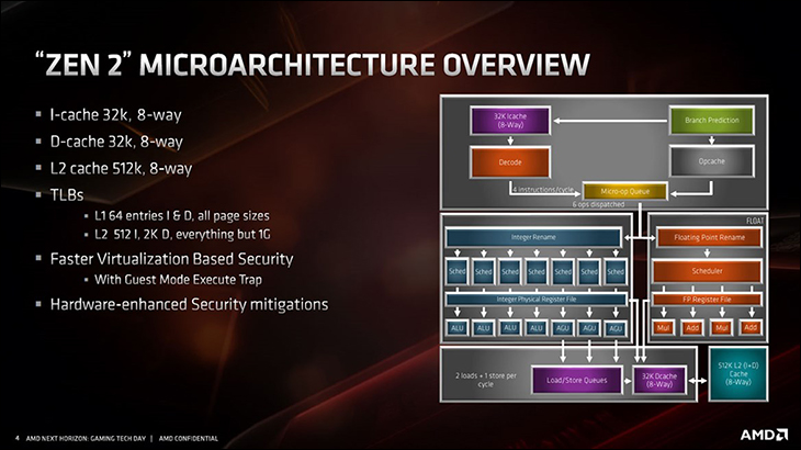
The L1 is still using a Branch Target Buffer as Zen 1 and Zen+ used, but it too is now doubled from 256 to 512 entries. Interestingly enough L1i cache is now only 32KB instead of 64KB per core like the previous Zen generation… but as it is 8-way instead of 4-way associative some of the difference is capacity is made up for in efficiency. Making up for this small loss in L1 instruction cache is macro-operation cache (MOP) has doubled to an impressive 4K. MOP cache allows the processor to decode complex operations into Macro-Operation code once, stick the answer in cache and then skip the decoding cycles when it encounters that operation in the future. The more cache, the more MOPs it saves, the more cycles it saves, the higher the IPC.
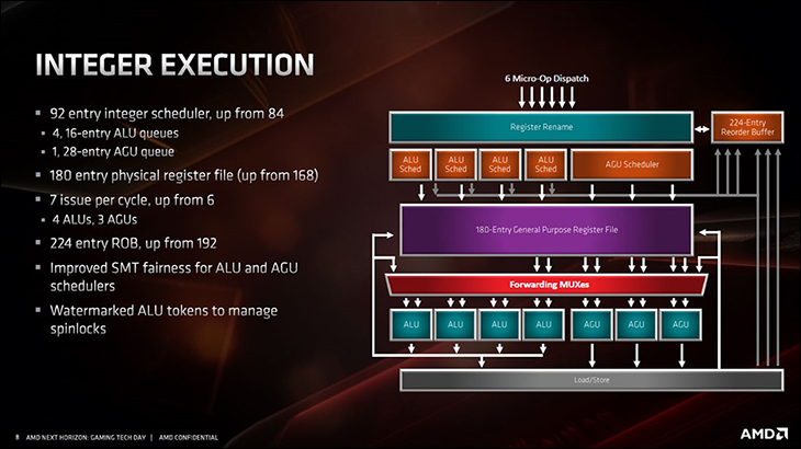
To further help IPC, AMD Zen 2 is now – finally- using a 256bit wide Floating Point Unit data path. Amongst other things (such as generating a single MOP instead of two for 256-bit instructions… and thus saving cycles and cache space) Zen 2 is now capable of handling ‘double-wide’ AVX-256 instructions in a single cycle. While this will not result in a doubling of AVX performance over original Zen models… it does indeed decrease wasted cycles. Once again improving overall performance. In this vein, FP multiplication latency has also been decreased from 4 cycles to 3 cycles.
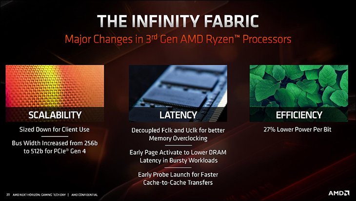
On top of all these low-level changes is another, one that everyone will be glad to see… and immediately grasp its impact. That is the Infinity Fabric interconnect. Due to its new chiplet configuration, even more data will be traveling the Infinity Fabric interconnect at any given time. This is just a fact of life for Zen 2 processors. With the last generation of Zen (be it Zen or Zen+) Infinity Fabric was a major bottleneck for a lot of users. To ensure that this increase in load does not result in bottlenecks, the all new ‘Infinity Fabric 2’ is a PCIe 4 based interconnect. This change means that even at the exact same frequency IF2’s bandwidth is double that of Zen 1 or Zen+. To be precise, instead of 256-bits wide it is now 512-bits wide. AMD also states they have improved the overall efficiency of IF2 by 27 percent, further decreasing bottlenecks on this critical interconnect.
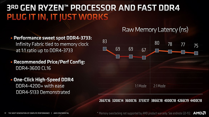
Also helping to alleviate concerns over this perceived handicap, IF2 has been decoupled from the memory clock. Though not entirely. At memory speed of DDR4-3733 (or 1866.5MHz for IF2) or lower, the IF2 and memory clock is linked at a 1:1 ratio. At above this it is a 2:1 ratio – with the IF2 running at half the memory clock. This certainly takes stress off the memory and IF2 controller when higher frequency memory is used, but even more careful consideration has to be paid to memory speed when selecting a DDR4 kit of RAM to pair with the new Ryzen 3 processors. For example, ultra ‘fast’ and expensive DDR4-4266 memory will result in IF2 bandwidth the same as if DDR4-2133 was used. AMD recommends DDR4-3600 or DDR4-3733 for this very reason. So, while the doubling of bandwidth from doubling the bit size of the IF2 will reduce bottlenecks it is not the slam dunk success it could have been if the Infinity Fabric 2 clock had been entirely decoupled from memory. It is however a great step in the right direction.
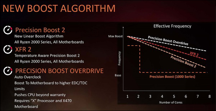
Another low-level improvement is in regards to how the processor handles frequencies. With Ryzen 1000-series certain models came with two specifications: those on the box, and an XFR boost rating which could boost above the specified maximum boost rating. With Zen+ based Ryzen 2000-series this prioritization on single thread performance was changed to overall performance. This was done via ‘Precision Boost’ which allowed the processor to have much more fine grain control over each of the core’s frequencies than the PBoost in Ryzen 1000-series CPUs.
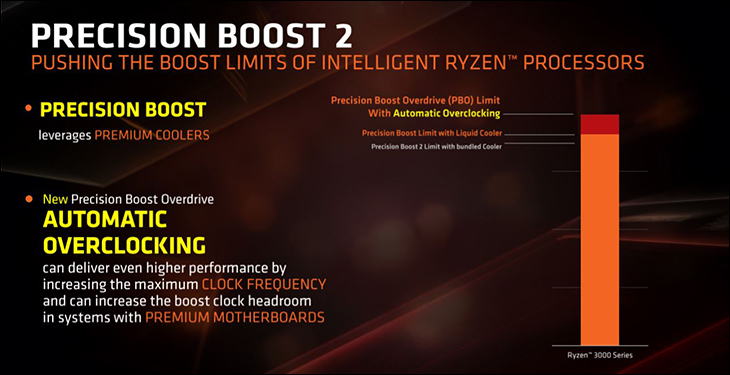
With Zen 2 based Ryzen 3000 series this Precision Boost feature has been further improved. Much like Precision Boost 1.0, Precision Boost 2.0 is an opportunistic algorithm which will actively monitor each core and provide additional frequency boost to those that need it. As with PB 1.0, it will do this in 1ms time slices. However, there is no longer a lower clock speed limit for when more than 2 cores are active. Instead, it looks at all the cores and as along as PPT (Package Power Tracking), TDC (Thermal Design Current), EDC (Electrical Design Current), and temperatures are within tolerances… it will work with each core to maximize all active cores’ frequencies. So, for example if three cores are active and three are not, the three non-active will have their frequency and power consumption drastically reduced and this additional overhead applied to the three active cores. Temperature though is actually the most critical deciding factor. If the CPU considers the temperatures are close to its TJMax it will not push the cores as hard. So, the cooler running the processor the harder it can push the active cores.
With that said, what it will not do under any circumstances is boost a core beyond the specified maximum frequency. In the Ryzen 5 3600X case this means no core will ever be pushed beyond 4.2GHz. However, it can – under some circumstances – push more than one core to this level… even all of them (though that is highly, highly… highly unlikely). Much like XFR/XFR2 and PB 1.0, the new Precision Boost 2 is enabled by default and works ‘out of the box’ with zero input needed from you. This is a nifty little feature that is very reminiscent on how modern video cards handle things internally.
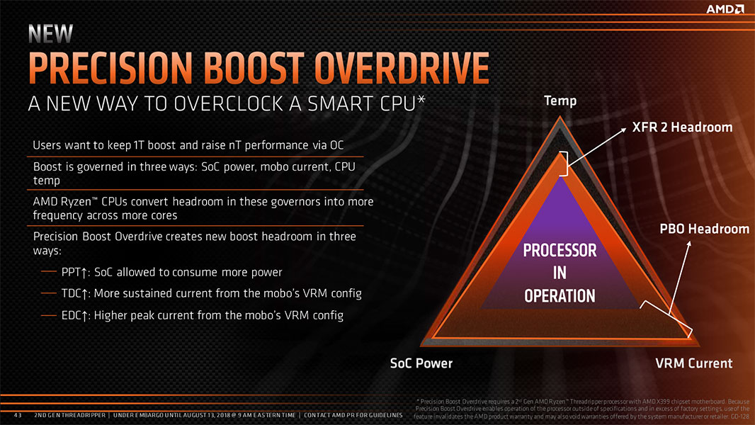
Also now include are two interesting features. The first is Precision Boost Overdrive (PBO), which made its debut last generation. Unlike PB, PBO has to manually enabled. PBO will push higher frequencies when the CPU is too hot BUT you cannot change the temp it considers to be ‘too hot’. So while PBO will give more performance to a hot running CPU than PB… it is not going to be night and day different. Instead where you will see the most impact is on cool running processors. Here it will boost overall performance by allowing ‘enhancements’ to the other three metrics the CPU uses in its calculations – max power consumption allowed for the socket and CPU (PPT), max sustained amps that can be pushed through a given mobo’s VRM/power delivery subsystem (TDC), and Electrical Desing Current (EDC).
Depending on how good the motherboard is, the BIOS may indeed contain options that are bordering on insane for these metrics… and allow you to tell the processor’s built in algorithms that it really is a more powerful/higher TDP/etc. processor than it really is. Just understand that temperatures are going to quickly skyrocket if you let PBO use the equivalent settings of a 195TDP chip on a 95TDP processor. Also do not be surprised if you see voltage peaks of 1.5v when you manually enabled PBO – so good after market cooling all but a requirement to successfully seeing a difference with PBO over PB. What also must be taken into consideration is PBO will void your warranty. Whether or not AMD can tell if you used PBO is another thing, but their literature is very specific. They consider PBO to be the same as manual overclocking.
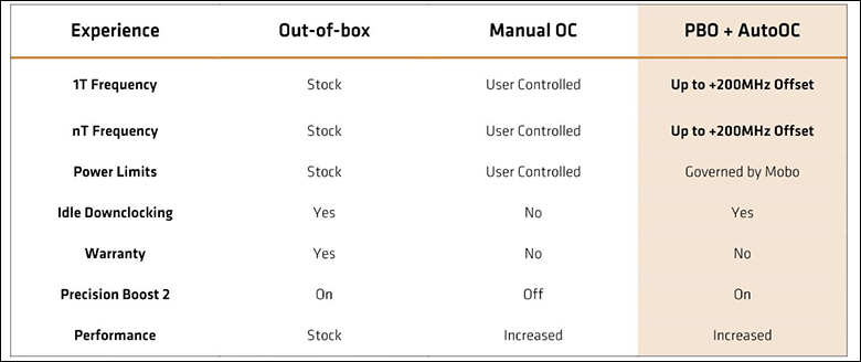
If all this is not confusing enough there is another new feature that sits on top (or at least to the side) of PBO. That is ‘autoOC’. AutoOC allows for upwards of 200Mhz over rated maximum boost frequency settings. It is not XFR. It will be applied to PBO and allow one or all cores to hit higher than the processors rated ‘maximum’ frequency. Though once again with all the limitations already listed taken into consideration before doing so. As such AutoOC will be of very limited value to those without great cooling solutions. So do not expect to see upwards of a 200Mhz boost outside of single active core / dual thread scenarios all that often. It too will also technically void your warranty.
Closer Look
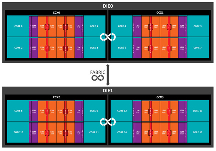
Before we start, it certainly has been awhile since home users have been exposed to Multi-Chip Module designs; however, it really is not all that surprising to see AMD go in this direction. After all, while their home user Ryzen processors were not MCM based, AMD’s very own ThreadRipper was right from the get go. They simply combined multiple ‘Ryzen’ chips on one PCB, included more logic and low-level controllers, created a bigger socket to handle it all… and called it good. With that said, even TR architecture did not take the MCM philosophy as far as AMD has with Zen 2… as ThreadRipper was just multiple-dies on one package.
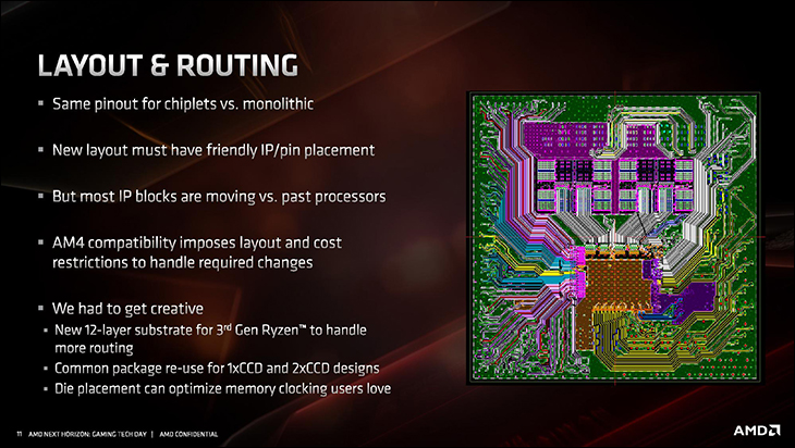
We have already gone over the various low-level improvements that Zen 2 brings to the table, but one key area we did just briefly touched on was the modularity of Zen 2. With the Ryzen 3000-series the entire architecture is built around having up to 3 chiplets on the ‘CPU’ printed circuit board. Even on the smaller ones, which only use 1 CCD and one cIOD chiplet, have all the tracings and pathways there for a second chiplet. This is because it is the same CPU printed circuit board with AM4 form-factor and pinouts used for all Ryzen 3000, Zen 2 processors.
This ‘recycling’ means noticeably lowered production costs across the entire Ryzen series. They simply have to mix and match CCDs and/or ‘GPU’ chiplets to create various price-point models. All on the same single fab’ed PCB. This cost savings on both the chiplets (vs CPU) fabbing and the PCB required for all Zen 2 based Ryzen 3000 models plays a large part in how AMD is easily able to offer a 6-core, 12-thread Ryzen 5 3600X for under $250. At this price point they are not only making a good profit but a great one… and can churn them out by the truck load. This should help alleviate potential price gauging by retailers over ‘sacristy’ excuses.
The downside is an inherent design limitation. Three chiplets means we will not be seeing larger that 16-core / 32 thread Ryzen 3000 series CPUs, nor will we see above 8-core/16-thread “APUs”… nor integrated graphic ‘APU’ models with onboard GDDR/HBM RAM. Anything above 2 chiplets for the processing cores will require an entirely new PCB and a special fabrication run just for them. Barring Intel pulling a massive rabbit out of their hats 16 cores is as big as Ryzen is going to get.
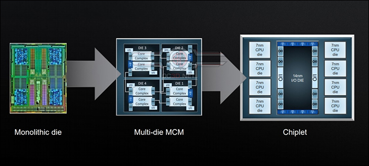
Turning to ‘old school’ MCM CPU architectural design is also arguably a short-term solution to a long-term problem. That problem is there is still only so much room on an AM4 sized CPU ‘PCB’ for so many chiplets. In fact, MCM and its ‘chiplets’ take up more room than a comparable ‘monolithic’ CPU design. Even reducing the node size below 7nm will only help so much. At a certain point AMD will have to start creating ‘3D’ or ‘stacked’ chiplet based designs. However, it is a lot easier to create a CCX stack than it is to create fully functioning CPU… and the cIOD chiplet certainly does not need to be a stacked design. This too is how future Zen 3/4/5/etc. AMD processors will be able to keep costs down while still being on the cutting edge of CPU architectural design. In the meantime, we will all just have to satisfy ourselves with a ‘mere’ 16 core mainstream processor… which up until Zen 2 would have been a HEDT / ThreadRipper socket-based model and an accompanying larger asking price.
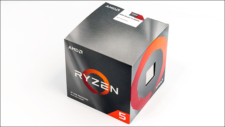
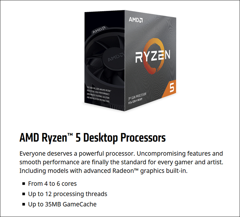
Moving on. AMD certainly does know how to create an excellent shipping container. We say this as the shipping container is colorful enough to be attention getting, without being off-putting. It clearly states exactly what model CPU is housed inside – so (sadly) you cannot use the excuse you picked up the ‘wrong box’ at the store and now since it is opened can’t be returned.
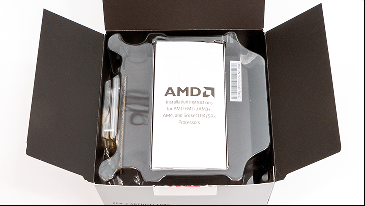
It even does a very good job of protecting the CPU – thanks to cardboard and clamshell protective layers.
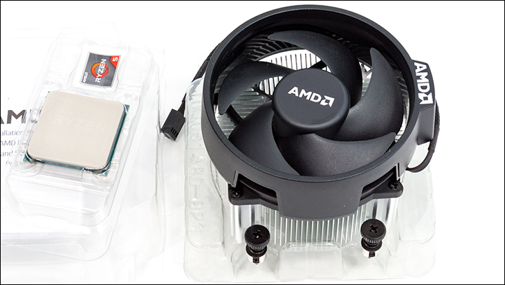
It even comes with a decent 95 watt TDP capable AMD Wraith Spire CPU cooling solution. The only minor issue is the Wraith Spire included is not the RGB enabled variant. Instead it just cools your CPU without adding any LEDs. On the positive side, this is a much more robust stock cooling solution than with ships with the non-X 5 3600 CPU (which gets the smaller 65TDP capable Wraith Stealth).
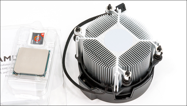
In other words, for fitty dollars extra buyers get a better CPU cooling solution and higher Precision Boost settings than opting for the less expensive 5 3600 CPU. For manual overclocking enthusiasts that is not going to be fifty dollars well spent. For everyone else it is a tough choice. PBO + autoOC + a good aftermarket cooling solution will net similar results… but PBO does technically void your warranty. Decide which is more important to you and choose accordingly.
In either case, both 5 3600’s are 6 core Zen 2 based processors with native SMT baked right in. This feature does put them ahead of the competition as Intel’s implementation of SMT (‘HyperThreading’) has not been implemented on their newer models. SMT does provide a minor performance boost, and does help improve overall CPU performance. Unless you are using the Ryzen series in a bank, the stock market… or the NSA, the minor decrease in security which accompanies SMT is not worth worrying about.
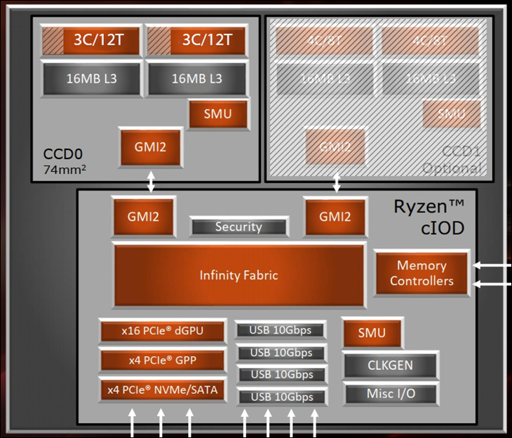
The next thing is since Zen 2 CCD’s are made up of 2 CCX’s with four cores each, at least one of the CCXs is one which failed 7 testing and has had at least one core disabled. AMD is mum on the precise configuration of deactivated to active cores in each CCX so there could be some random combination – or ‘CPU lottery’ – involved. Most likely though the 5 3600X will have two CCXs with a single core deactivated. This would give a better balance of L3 cache for all active cores vs. having a fully enabled CCX sharing 16MB of cache and then two cores in the second CCX sharing the other 16MB of cache. The end result in both scenarios though will be the same: 6 active cores capable of 12 threads, backstopped by a total of 32MB of L3 cache.
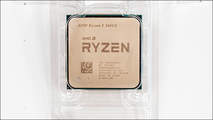
While the Ryzen 5 3600 comes with clock speed ratings of 3.6Ghz/4.2Ghz the Ryzen 5 3600X comes with them set to 3.8Ghz to 4.4Ghz. This represents an across the board 200Mhz improvement over the frequency settings of the Ryzen 5 2600X (3.6/4.2) and Ryzen 5 1600X (also 3.6 – 4.2). Equally impressive it is rather comparable to the Intel Core i5-9600K (a 6c/6t processor) with a base frequency of 3.7Ghz and a max boost of 4.6Ghz. What is not comparable across previous Ryzen or Intel processors is the amount of cache the Ryzen 5 3600X has on tap. Instead of 9MB (9600K) or even 16MB of L3 cache(2600X) the Ryzen 5 3600X has 32MB of L3 cache. Instead of 1.5MB (9600K) it has 3MB of L2 cache (though this is the same amount as the Ryzen 5 2600X). The only reduction is in L1 which is now 384KB (same as 9600K) instead of 576KB… but it is 8-way and not 4-way associative, which does make a big difference.
When you take in the various low-level improvements the Ryzen 5 3600X is a downright massive improvement over the Zen+ based Ryzen 5 2600X it replaces. The very fact it can do this and still be somewhat backwards compatible with older motherboards is phenomenal. Hopefully Intel follows suit ASAP and we get to see multiple generations of CPUs with backwards compatibility from both manufactures. In the meantime, AMD is certainly keeping their promise of pushing the boundaries without pushing expensive socket upgrades on the buying public.
Test Bed
Ryzen 1000-series Testbed:
• Motherboard: ASUS RoG STRIX X370-F Gaming
• CPU: AMD Ryzen 5/7
• RAM: 16GB Crucial Ballistix Elite DDR4-3200
• Cooling: Corsair H115i w/ 4 fans
• Video Card(s): MSI GTX 980Ti Lightning
• SSD: 1x Crucial MX500 1TB
• Power Supply: Corsair AX860i
Ryzen 2000-series Testbed:
• Motherboard: ASUS RoG STRIX X470-F Gaming
• CPU: AMD Ryzen 5 2000-series
• RAM: 16GB Crucial Ballistix Elite DDR4-3200
• Cooling: Corsair H115i w/ 4 fans
• Video Card(s): MSI GTX 980Ti Lightning
• SSD: 1x Crucial MX500 1TB
• Power Supply: Corsair AX860i
Ryzen 3000-series Testbed:
• Motherboard: ASRock X570 PHANTOM GAMING 4
• CPU: AMD Ryzen 5 3000-series
• RAM: 16GB Ballistix Elite DDR4-3600
• Cooling: Corsair H115i w/ 4 fans
• Video Card(s): MSI GTX 980Ti Lightning
• SSD: 1x Crucial MX500 1TB
• Power Supply: Corsair AX860i
Intel LGA 2011-v3 Testbed:
• Motherboard: Asus TUF X99 Mark 1
• Processor: Intel (various)
• Memory: 32GB GSkill TridentX DD3-2400 4x8GB
• Cooling: EVGA CLC 280 AIO
• Video Card(s): MSI GTX 980Ti Lightning
• SSD: 1x Crucial MX500 1TB
• Power Supply: Corsair AX860i
Intel LGA 1151-200 Testbed:
• Motherboard: ASUS RoG STRIX Z370-E Gaming
• CPU: Intel 7-series (various)
• RAM: 16GB Ballistix Elite DDR4-3600
• Cooling: Corsair H115i w/ 4 fans
• Video Card(s): MSI GTX 980Ti Lightning
• SSD: 1x Crucial MX500 1TB
• Power Supply: Corsair AX860i
Intel LGA 1151-300 Testbed:
• Motherboard: ASUS TUF Z370-Pro Gaming
• CPU: Intel 8-series (various)
• RAM: 16GB Ballistix Elite DDR4-3600
• Cooling: Corsair H115i w/ 4 fans
• Video Card(s): MSI GTX 980Ti Lightning
• SSD: 1x Crucial MX500 1TB
• Power Supply: Corsair AX860i
Overclocking
With every generation of CPU’s released the benefit vs. time investment ratio does get slightly worse. This is because AMD and Intel have been implementing more and more features that were once the sole domain of video cards. For all intents and purposes, modern CPUs do a lot of ‘automatic’ overclocking. So much so it is quickly getting to the point where manual overclocking is becoming less and less useful for the typical buying public. This is not to say there are no benefits, but it really will depend on your work loads and how many cores you routinely are maxing out at any given time. This is especially true of this third generation of Ryzen processors. Their ‘out of the box’ abilities, especially when combined with PBO and autoOC, make it difficult to recommend taking the time to manually overclock them. The improvements are really not there, and instead AMD has already unlocked the majority of their potential… or atleast unlocked most of their potential this side of EZ-bake oven temperatures.
With that said it is still fun thing to do… and can actually increase the longevity of your CPU. Yes, in a rather ironic reversal AMD’s PBO (especially on aggressively set motherboards) will routinely hit 1.5 volts of power. That is a wee bit more than we are personally comfortable with – and probably explains why AMD considers their very own Power Boost Overdrive option a warranty voiding configuration. Instead we prefer to see things in the 1.4 range as a more… comfortable long-term overclock voltage range. With this in mind we hit 4.2 all core overclock that was 100 percent stable, and by pushing things up a tad to 1.43volts got 4.3Ghz all core overclock stable. Yes, this is technically less than the ‘stock’ 4.4Ghz boost… but it is doing it on all cores not just one thread. For a general purpose usage scenarios this 4.3 vs 4.4 is a noticeable improvement. For those who lightly use their system the opposite will be true. Only you can decide what is right for your needs. We would however be very tempted to leave it at stock for a while and see if you need more power before manually overclocking your shiny new Ryzen 3000-series CPU.
The one area that should be done is memory ‘overclocking’. It certainly is true that the stock DDR4-3200 configuration is a boat load better than the original Ryzen or even Ryzen 2000-series but… there is still a lot of gas left in the tank of this new cIOD memory controller. Hitting DDR4-3600 was a breeze. This is not something that we could say about Ryzen 1000 or Ryzen 2000 series CPUs. AMD really has gotten a handle of their memory controller issues and it shows. As such, even if you just leave the CPU in stock config… at the very, very least enable the XMP. Our recommendation is to buy fast memory and push it hard. Even the near entry level 3600X can take it. This new chiplet IO is that much improved over previous Ryzen generations.
Adobe Performance
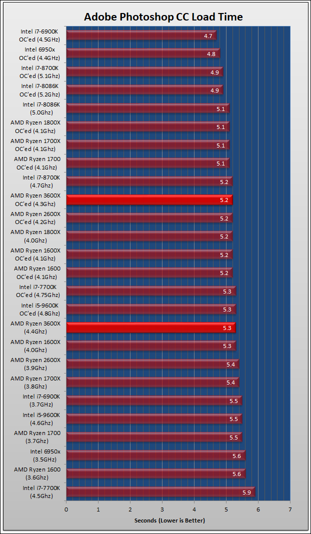
Adobe Photoshop CC 2017
Adobe Photoshop is a raster graphics editor developed and published by Adobe Systems for macOS and Windows. To further make loading slower we have included a bunch of extra brushes that need to be loaded before the program is ready to use.
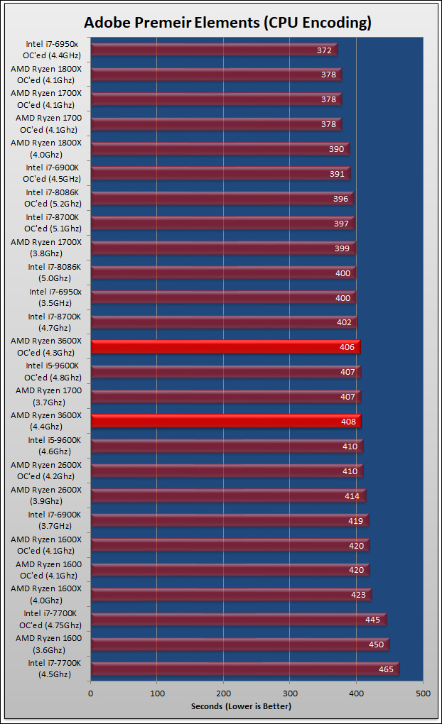
Adobe Premiere Elements 2015
Adobe Premiere Elements is a video editing software published by Adobe Systems. It is a scaled-down version of Adobe Premiere Pro and is tailored to novice editors and consumers. The entry screen offers clip organization, editing and auto-movie generation options. To stress the CPU we have disabled GPU rendering and instead Premier will use the CPU only.
Cinebench & Geekbench Results
CINEBENCH R15 & R20
CINEBENCH is a real-world cross platform test suite that evaluates your computer’s performance capabilities. CINEBENCH is based on MAXON’s award-winning animation software CINEMA 4D, which is used extensively by studios and production houses worldwide for 3D content creation.
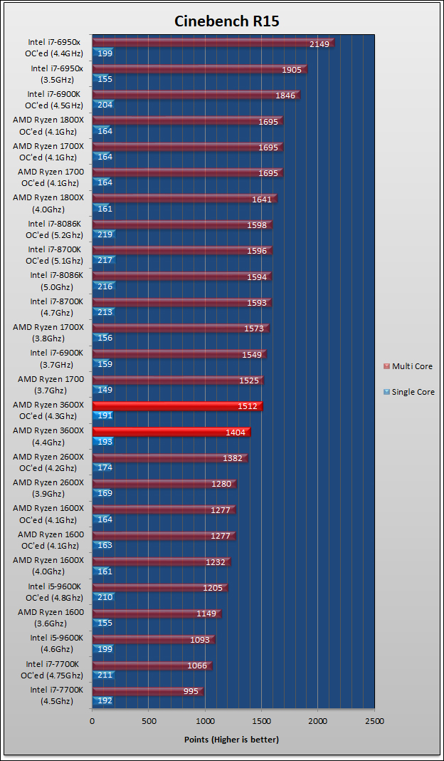
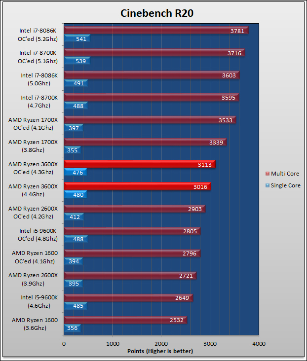
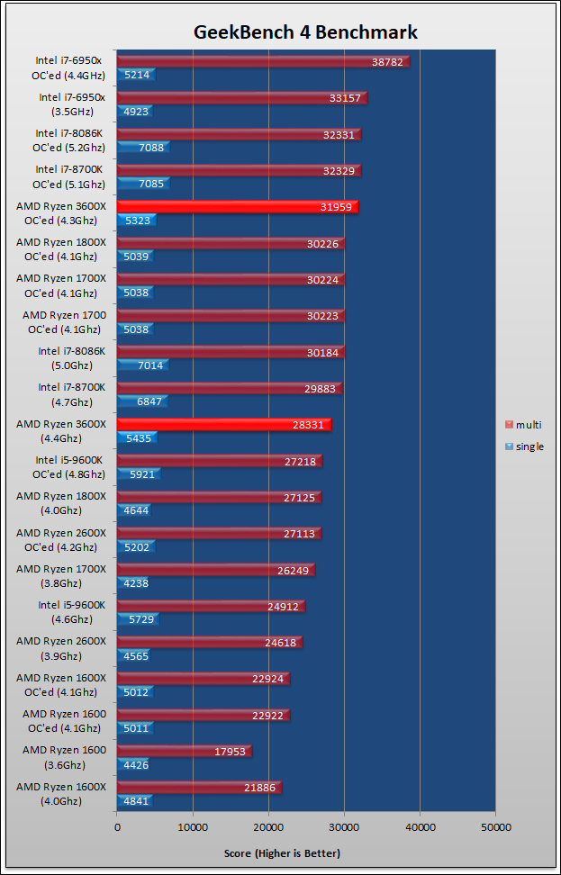
GeekBench Benchmark
Geekbench is a cross-platform processor benchmark, with a scoring system that separates single-core and multi-core performance,[1
[2
and workloads that simulate real-world scenarios
PCMark, POV-Ray, Blender
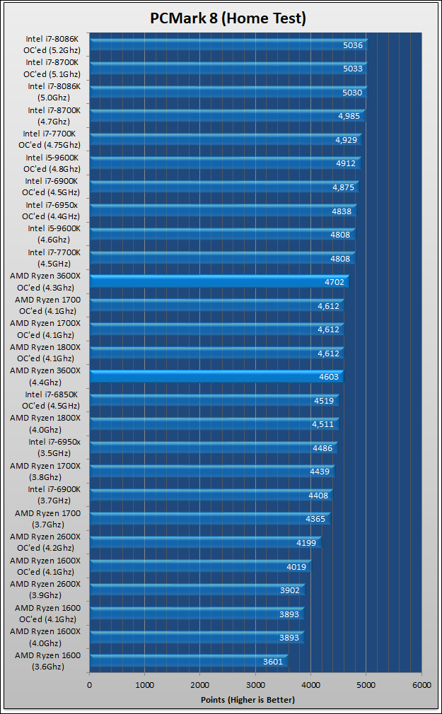
PC Mark 8
PCMark is a computer benchmark tool developed by Futuremark to test the performance of a PC at the system and component level. In most cases the tests in PCMark are designed to represent typical home user workloads.
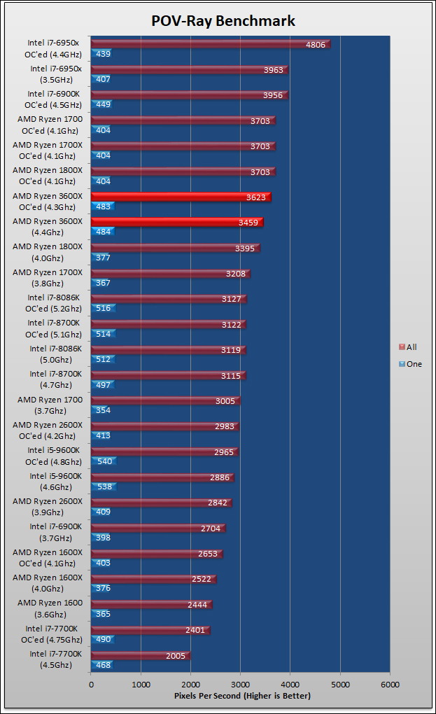
POV-Ray Benchmark
The Persistence of Vision Ray Tracer, or POV-Ray, is a ray tracing program which generates images from a text-based scene description, and is available for a variety of computer platforms.
Blender Benchmark
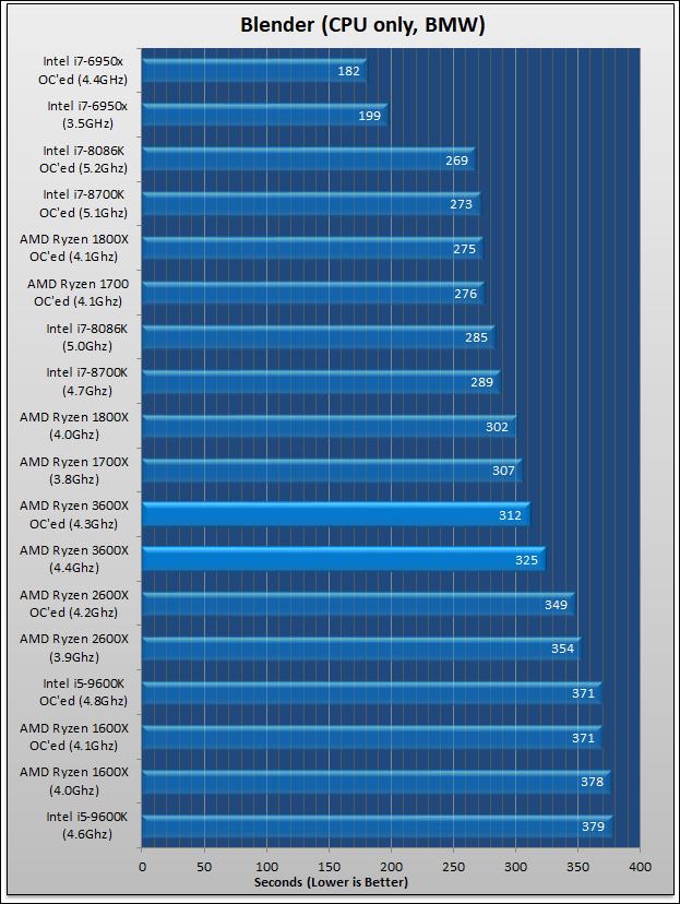
Blender is a free and open-source 3D computer graphics software toolset used for creating animated films, visual effects, art, 3D printed models, interactive 3D applications and video games. Also included is a CPU benchmark Utilty. For testing we have opted for the standard ‘BMW’ demo.
winRAR and TrueCrypt
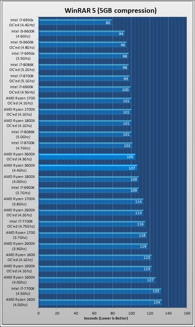
winRAR Benchmark
WinRAR is a popular file compression and decompression tool that also happens to be multi-threaded application. While it does have a built in benchmark we have opted to use a custom 5GB test consisting of small, medium, and moderately large files. We then time how long it takes to compress the files into one .rar file with all WinRAR settings left at their defaults.
TrueCrypt AES Benchmark
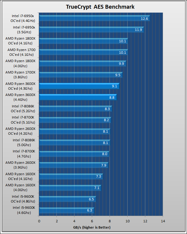
TrueCrypt is a discontinued source-available freeware utility used for on-the-fly encryption (OTFE). It can create a virtual encrypted disk within a file, or encrypt a partition or the whole storage device (pre-boot authentication). While discontinued its built-in benchmark using AES is still extremely relevant. Included result is the average of both encryption and decryption performance
x264 HD and Handbrake
x264 HD Benchmark
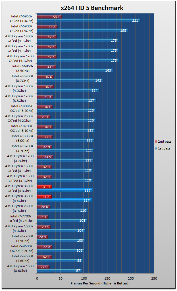
x264 HD Benchmark is a benchmark that allows you to measure how fast your PC can encode a 1080p video clip into a high quality x264 video file. It allows for an easy comparison because everyone running it will use the same video clip and software. The x264 video encoder has a fairly accurate internal benchmark (in frames per second) for each pass of the video encode and it also uses multi-core processors very efficiently. All these factors make the x264 HD Benchmark an ideal tool in comparing the video encoding performance of different processors and systems.
Handbrake X265
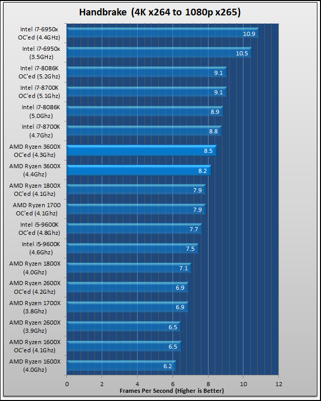
HandBrake is a free and open-source transcoder for digital video files, originally developed in 2003 by Eric Petit. Since then it has continued to evolve. Included in its list of features is the ability to transcode existing video from x264/MPEG-4 AVC to x265/HEVC. For this test we are using a one hour length 4K x264 file and using the H.265 MKV 1080p30 preset transcoding it to 1080p resolution.
AC:S & BF4
Assassins Creed: Syndicate Gaming Benchmark
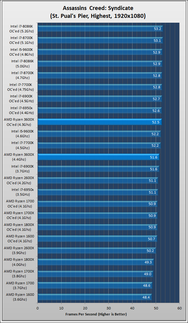
Assassins Creed: Syndicate is an historical action-adventure video game, published by Ubisoft and released in October 2015. Like Battlefield 4 this games does not include an in-game benchmark. This makes it perfect for more real world gaming testing. To obtain repeatable results we have used FRAPs and recorded a custom run through Thames River section starting on St. Pual’s Pier. An average of four runs was taken.
The settings used in the testing below are stock highest settings for quality, VSync disabled and a resolution of 1920×1080.
Battlefield 4
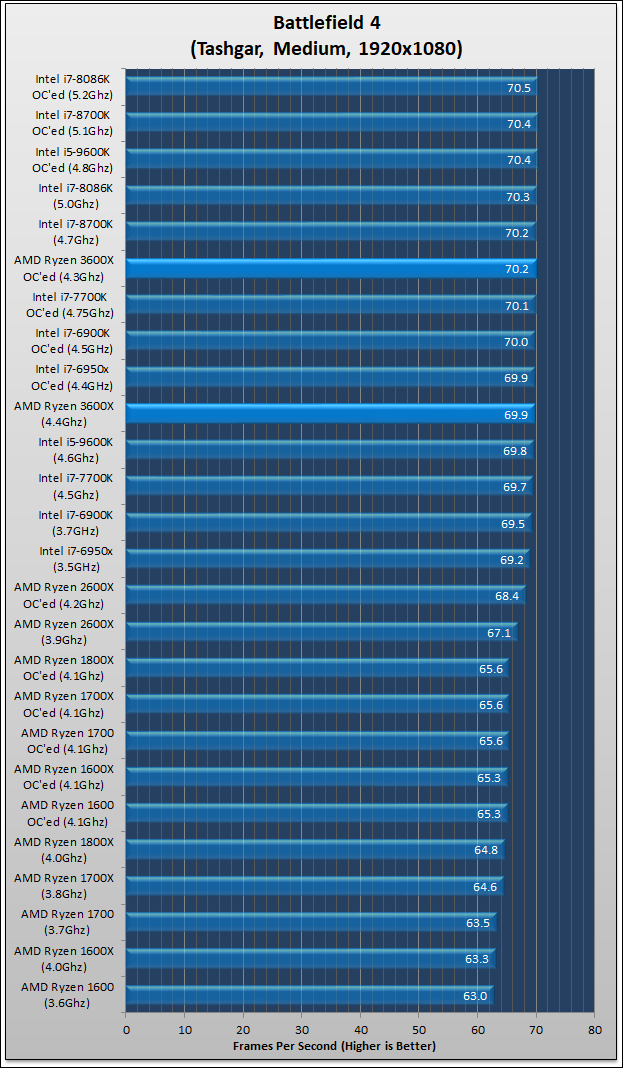
Battlefield 4 is first person shooter video game, published by EA Digital Illusions CE and released in October 2013. Unlike most, this games does not include an in-game benchmark. This makes it perfect for more real world gaming tests. To obtain repeatable results we have used FRAPs and recorded the first 90 seconds of the single player Tashgar level. An average of four runs was taken.
The settings used in the testing below are Ultra pre-set for quality, with VSync disabled and a resolution of 1920×1080.
Crysis 3, GTA V, Metro LL
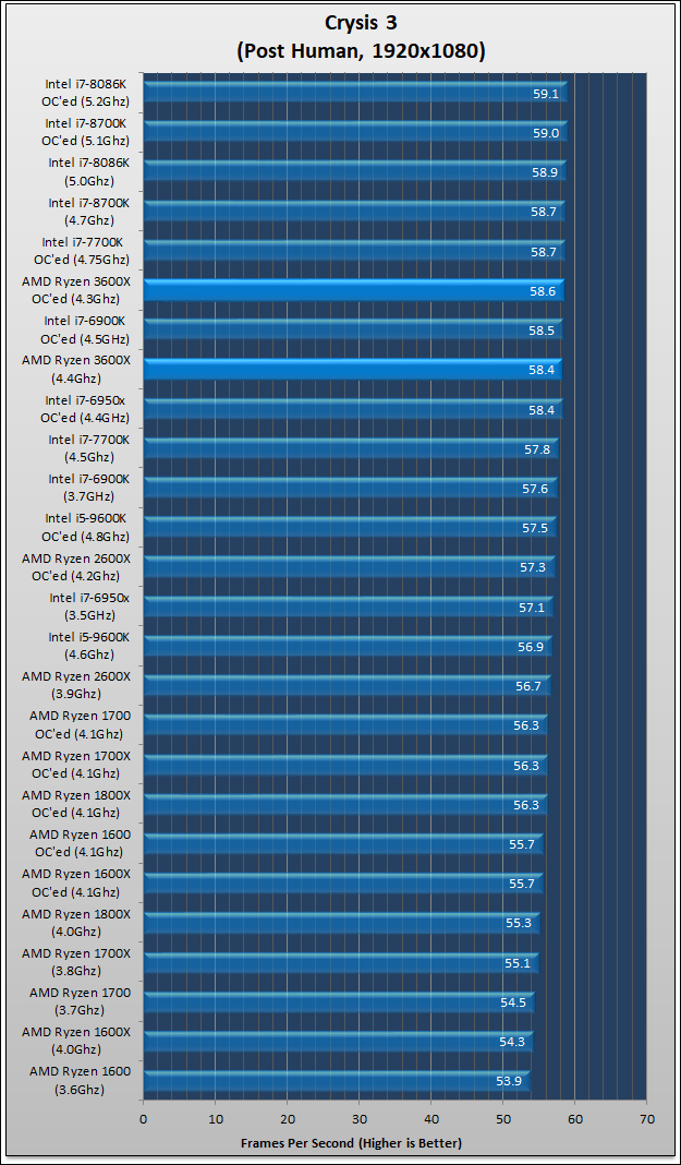
Crysis 3 Gaming Benchmark
Crysis 3 is a first person shooter video game, published by Electronic Arts and released in February 2013. While older than some of the others it is one of the most visually stunning games released to date and puts a lot of demands on the GPU. This makes it perfect for more real world gaming testing. To obtain repeatable results we have used FRAPs and recorded 90 seconds of the single player ‘Post Human’ level, starting as soon as soon as prophet is handed a Hammer II pistol by Psycho. An average of four runs was taken.
The settings used in the testing below are highest settings for quality, VSync disabled and a resolution of 1920×1080. Texture Quality, Game Effects, Objects, Particles, Post Processing, Shadows, Shading, Water, and System Specs all set to Very High. Motion Blur was set to High and Lens Flare was set to On. Anti-Aliasing was set to MSAA 8X and Antistrophic Filtering was set to 16x.
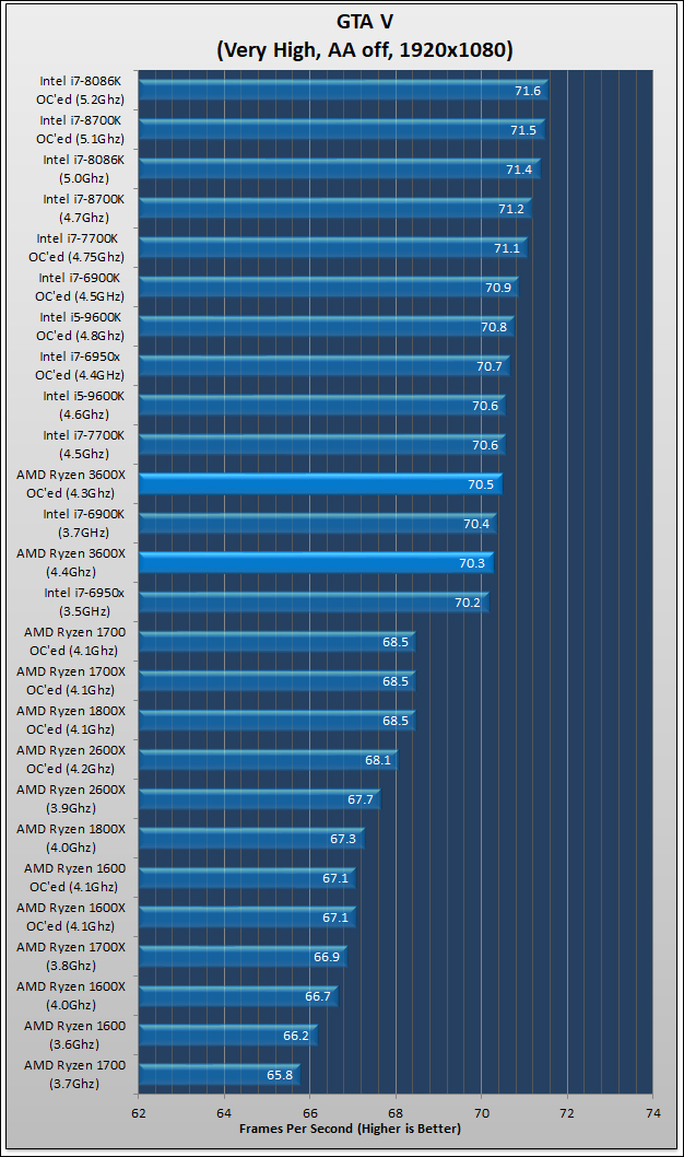
Grand Theft Auto 5 Gaming Benchmark
GTA V is an open world action-adventure video game published by Rockstar Games and released in April 2014 for the PC. The game has a benchmark component to it that mimics game play and an average of four runs was taken.
The settings used in the testing below are stock ‘very high’ settings for quality, VSync disabled and AA set to off, with a resolution of 1920×1080.
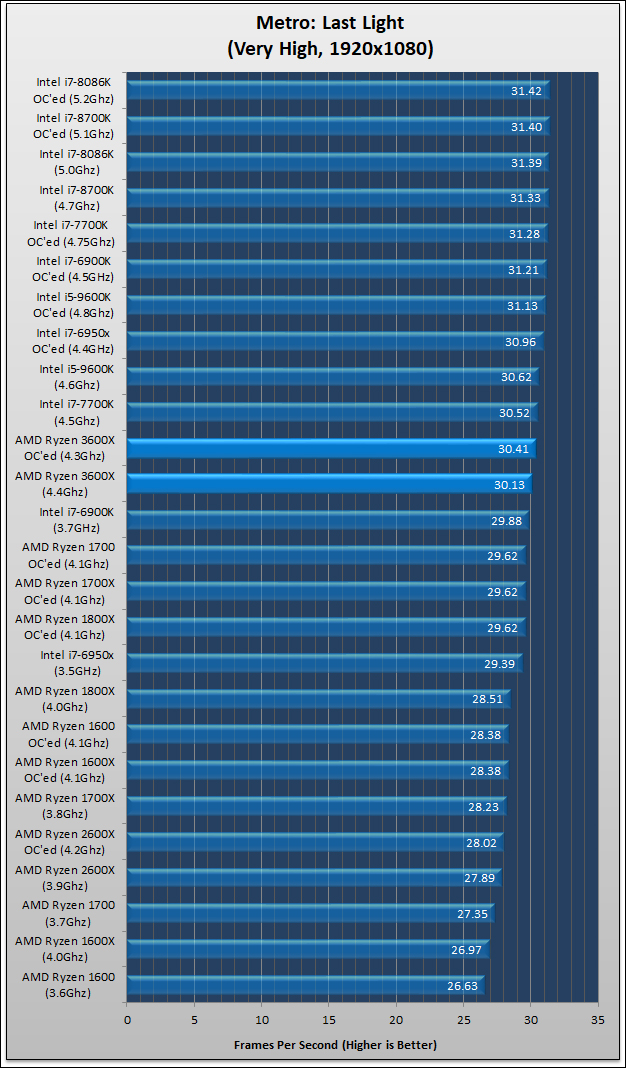
Metro: Last Light Gaming Benchmark
Metro: Last Light is a DX11 first-person shooter video game developed by Ukrainian studio 4A Games and published by Deep Silver released in May 2013. The game is set in a post-apocalyptic world and features action-oriented gameplay. The game has a benchmark component to it that mimics game play. Scene D6 was used and an average of four runs was taken.
The settings used in the testing below are Very High for quality and a resolution of 1920×1080. DirectX 11 is used, texture filtering is set to AF 16X, motion blur is normal, SSA turned on and tessellation is set to high.
Score Card and Summary
Performance: 34 out of 40
Ryzen 3000-series CPUs, even ‘little ones like the 5 3600X, do have thermal limiting related issues when it comes to multi-core performance. However, the new Zen 2 is much better than its predecessors in this regards. With good cooling they are rather potent. Just be ware that you will need good cooling to see their full potential – the stock cooler will not cut it.
Ease of Use: 19 out of 20
Precision Boost 2 works marvelously well… and does its ‘magic’ seamlessly and automatically. Mix in a dramatically improved memory controller, though we still recommend Samsung b-dies for optimal results, and the end result is the easiest to use Ryzen processor to date. If PBO and autoOC were enabled ‘automagically’ instead of manually it would be darn near perfect.
Innovation: 20 out of 20
With Zen 2 AMD is literally rewriting the manual for how to create high performance multi-core processors. The only possible way the new Ryzen series could have improved upon this massive upgrade was to also include 3D or ‘stacked’ core architecture. That probably will be Zen 3. In the meantime, the new Ryzen 3000-series makes Intel’s monolithic design look outdated in comparison.
Value: 19 out of 20
It really… really is hard to argue with a 6 core, 12 thread processor that outmuscles processors which cost upwards of 40 percent more. The only weak link is slightly reduced gaming performance, though even here AMD has closed the gap with Intel and makes recommending the Intel Core i5-9600K rather difficult to say the least.
Final Score: 92 out 100
It may not be perfect, and has a tendency to run hot, but the Ryzen 5 3600X is not only a marvelous upgrade over the Ryzen 5 2600X it is also a great sign of things to come. Zen 2 is the real deal, and once AMD gets a handle on voltages and low-level refinements Zen 2 is going to prove to be the future of CPU design. In the mean time it gives both a great glimpse of things to come while also being a great value CPU right now. That is indeed an impressive combination.
Closing Thoughts
With Zen 2 AMD has indeed created another paradigm shifting architecture. One that tips ‘common wisdom’ on its head. Up until now ‘common wisdom’ said that multi-chip module designs were difficult and risky propositions. After all, the last ‘great’ example of MCM in consumer CPUs was Intel’s Core 2 Quad ‘space heaters’. AMD’s Zen 2 architecture is no Core 2 Quad. It is the modern-day equivalent of AMD’s Athlon 64 X2 series which rocked the world and put multi-core CPUs on the map. Did AMD just get lucky by releasing it now while Intel is having so much fabrication production problems? No. Roman Philosopher Seneca said it best: “Luck is what happens when preparation meets opportunity”. AMD’s design team dared to think outside the box so soon after their smashing success of Zen, and AMD is now going to reap years of rewards from willingness to embrace the very essence of innovation.
It is also pretty obvious that AMD did not create their new Zen 2 architecture with the 6 core Ryzen 5 in mind. They did not even have 8 core models in mind. Instead of thinking small, Zen 2 was built around scaling well beyond 8 cores. Scaling in a sensible manner which did not trade performance for core count. To do this they took all they learned from ThreadRipper and created a new architecture which can, and will, scale up well beyond one or two CCD chiplets. This makes Zen 2 almost less than perfect for a single or even dual CCD chiplet based processor models. With only a single chiplet, especially one with half of a CCX’s cores disabled, the Ryzen 5 3600X certainly does not showcase what this new architecture can truly do.
Instead, what the Ryzen 5 3600X proves is that AMD has indeed come a long way on the efficiency of their processor design. While it is pushing it to call it parity with Intel in IPC, the differences are not all that large anymore. The end result is the Ryzen 5 3600X does not need to rely upon more cores to outmuscle its direct Intel competition. Instead it can do so in (near) apples to apples comparison. Unfortunately, Ryzen still does not scale as high as Intel can. Some of this is due to how hot this new MCM design gets when it gets above low 4GHz range. Some is due to unrefined software and how much voltage it is pushing to the cores. Some of it is software has not been optimized for MCM technology. The actual reasons do not matter, as the end result is the same: AMD is still trailing Intel in the shear frequency department.
Should this matter to you? That is where things get very interesting. At the time of writing the main competition for the Ryzen 5 3600X is technically Intel’s Core i5-9500, but in reality, it is the Core i5-9600K… which you can actually buy right now. The Ryzen 5 3600X has an MSRP of $249 (USD), whereas Intel’s offering will cost about $350 (USD). For the additional $100 buyers get 200Mhz higher single active core frequency boost (4.6Ghz vs 4.4Ghz). This translates to a real-world difference of about 250-300Mhz’ish in single threaded applications. When all cores are active… the opposite is true. The less costly Ryzen 5 3600X comes with 100Mhz of additional processing power – 3.8Gh vs 3.7Ghz and twice the number of threads (12 vs 6)… yet costs noticeably less than Intel’s offering.
When you add in the additional value-added features such as native PCIe 4 support to the equation the choice is clear. The Ryzen 5 3600X is an incredible value. One where you can almost get a ‘free’ motherboard for the same amount of money Intel’s 6-core / 6-thread mainstream CPU will set buyers back (e.g. the ASRock used in testing was only 155 USD). For this reason alone, AMD obviously succeed at their goal of market dominance in this corner of the marketplace.
Even PC gaming enthusiasts who are mainly concerned with ‘single core’ performance need to think long and hard before discounting this new AMD CPU. Yes, if you upgrade your gaming rig every year, or even 18 months, PCIe 4 will not matter… but what about two or three years from now when NVIDA and AMD both (probably) have PCIe 4.0 video cards out? Video cards which will never run at their full potential on Intel PCIe 3.0 motherboards. That slim advantage Intel has right now suddenly does not seem all that great a proposition now does it?
No matter what you decide the AMD 5 3600X does deserve careful consideration. Congratulations AMD for not only redefining how a modern CPU will be made from now on, but doing so in such a manner that does not impact value.

