Let us be perfectly clear. AMD’s Zen 1 / Ryzen 1000-series was a paradigm shift for how CPUs were created. By moving away from ‘monolithic’ CPU design to a building block design the ramifications of this innovation are still be felt today in the industry. So much so Intel hired ex-AMD employees to help create their own take on ‘Lego block’ design.
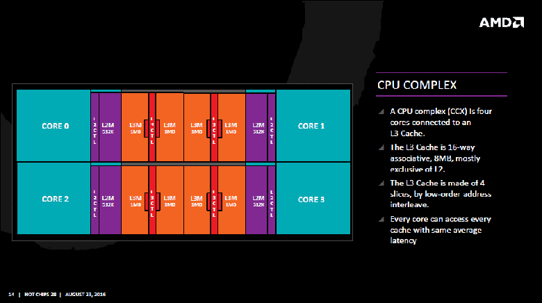
As a brief overview, Zen 1 architecture was based around the idea of Core Complex (CCX) ‘blocks’. These blocks contained four ‘cores’ (with anywhere from 0 to 2 of them deactivated), the memory controller, the IO controller, various L1-L3 cache, etc. The more CCXs you add to a ‘CPU’ the more powerful the end result is. This is why many refer to them as ‘Lego Blocks’. Of course, as these CCX blocks need to communicate not only with the rest of the system (e.g. the RAM or PCIe bus, etc. etc.) but also with other CCX’s AMD upgraded/revised their HyperTransport Interconnect technology to handle this increase in load. The end result is the Infinity Fabric that consists of two separate communication planes: Scalable Data Fabric (SDF) and Scalable Control Fabric (SCF). As the name suggests SDF portion of Infinity Fabric handles communications with the rest of your system, whereas SCF handles inter-CCX communications.
This combination was ingenious as it allowed AMD to easily scale up or down an entire product line-up, use more of the fabrication wafer (as a ‘bad’ CCX could be usually salvaged for lower Ryzen / ThreadRipper ‘CPUs”), and even easily create models with integrated graphic (what AMD calls “APUs” denoted by having a ‘G’ at the end of the model). This increased flexibility also allowed AMD the ability to not only create higher core count CPUs than Intel, but be much more agile in reacting to changing market demands.
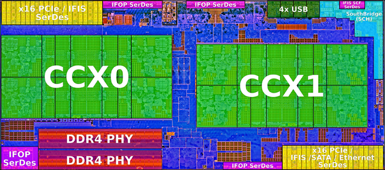
The downside is this design may be modular but is still based upon fully functioning, highly complex CCX’s which required a lot of die space for secondary controllers. Each CCX needed everything from integrated memory controllers on down, and are basically miniature “monolithic” Central Processing Units… just ones created and used in a radically different manner.
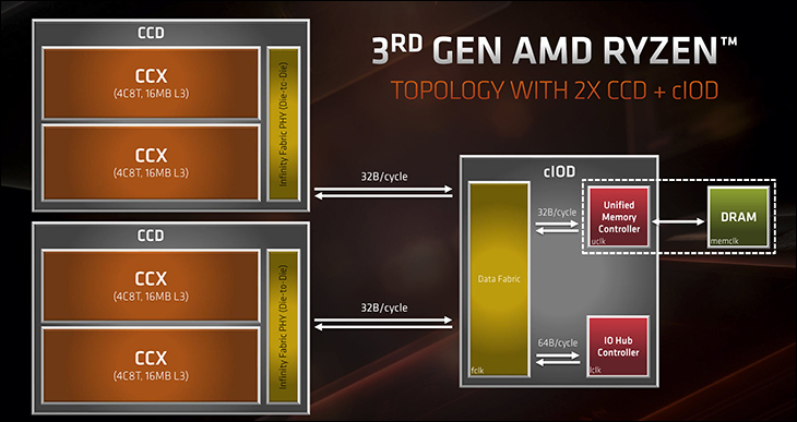
This is how Zen and Zen+ processors were all designed. Zen 2 / Ryzen 3000-series does things drastically different. Instead of designing CCX ‘blocks’ that do everything, AMD has split the processor design into two separate and distinct portions – or in more technical terms a “multi-chip module” (MCM) design.
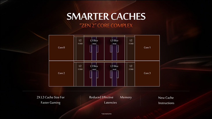
The first is a ‘chiplet’, called a “Chiplet Core Die” (sometimes referred to as a “Client Compute Die”) or ‘CCD’ for short. A CCD houses two noticeably less complex CCX groups of four processing cores (of which an entire CCX or even just core(s) in a CCX can be disabled). These new CCXs only contain the cores, L1/L2/L3 cache, and Infinity Fabric 2 pathways to connect the cores to the other new chiplet introduced with Zen 2. No memory controller. No inter-CCD communication pathways. Nothing else beyond what is needed to crunch numbers and talk directly to the other new chiplet.
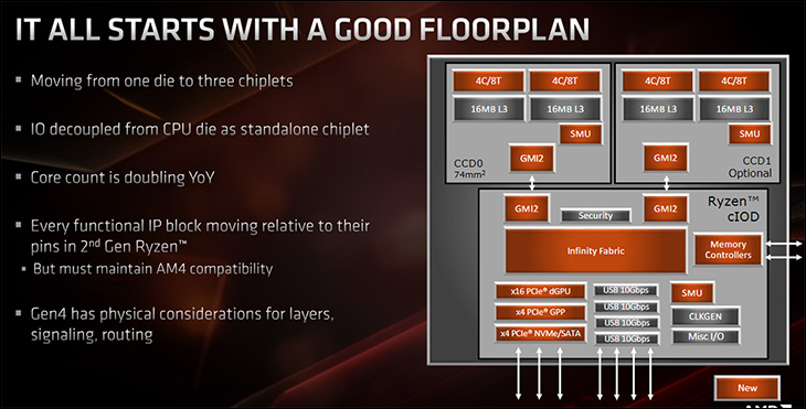
The second portion is an aptly named chiplet I/O Die – or ‘cIOD’ for short. This separate die on the MCM package (or “CPU”) is the central processing hub responsible for all the various portions which used to be housed inside the CCX. Including the SDF and SCF “Infinity Fabric 2” controller. In simplistic terms one can consider this IO chiplet as the middle man that handles all the low level I/O grunt work, allowing the CCX cores in the CCD to actually worry about just crunching numbers.
This change does numerous things, but the largest is it allows AMD the luxury of not having to build complex building blocks and then fail complex building blocks just because of a fabrication error in the memory or other secondary controller transistors. Instead they can create more chiplets per wafer and fail fewer of them. Equally important by removing these portions of the ‘classic’ CCX, this in turn frees up space for more important things like doubling the L3 cache from 8MB per CCX to 16MB (or 32MB per chiplet… even if the entire chiplet’s cores are not enabled – e.g. 3900X has 64MB with only a chiplet and half worth of CCXs enabled).
This removal of components from the CCX also means that Zen 2 is a Uniform Memory Access (UMA) based system not Non-uniform Memory Access (NUMA) like Zen 1 and Zen+. Questions over NUMA vs UMA for home users is really a non-issue. Both have their positives and negatives. For example, NUMA can result in lowered RAM latency in best case scenarios, but can result in rather high and rather random latency peaks. In the server world, NUMA is a four-letter word for high performance applications which demands consistent low latency results. Work arounds have been done via software to minimize this issue, but UMA does not have it. With UMA all cores access the same memory controllers, resulting in a more consent average latency. Thus Zen 2 in the server market is going to be a very big deal… but for home users it really is not that big a deal.
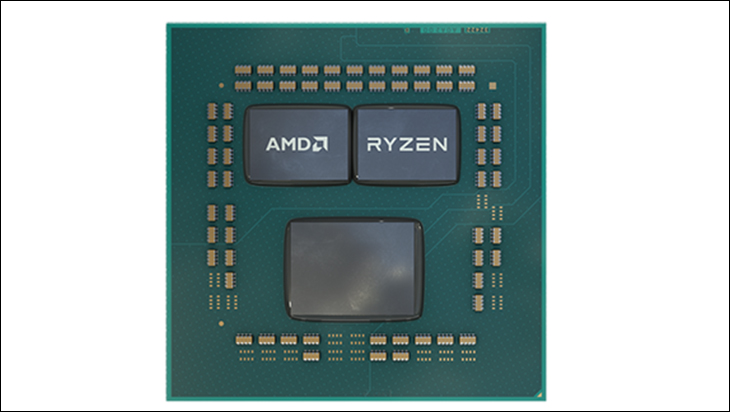
This new multi-chiplet design also allows AMD the luxury of not wasting 7nm fabrication time, or space, on secondary controllers which do not need this expensive fabrication node. Instead, the IO chiplet is being built on an older and less expensive 12nm fabrication process. This not only decreases the overall build cost of a Zen 2 based CPU, but also allows them to upgrade the IO chiplet’s features without “throwing out” any of the expensive 7nm processing chiplets already fabbed.
The downside, is by offloading the low-level controller to a secondary chiplet, the CCDs can no longer communicate directly with other CCDs. For processors which only house one CCD and one cIOD chiplet this is a moot issue; however, the 12 core R9 3900X and R9 3950X house two CCD’s. This means inter-chiplet data sharing has to not only cross the Infinity Fabric bus twice but also has be processed through the IO chiplet before reaching the other CCD. This will increase latency, but it is more of an edge case. One which will not happen all that often in home user scenarios. This is thanks to upgrades in the processor scheduler and predictive math algorithms which were enhanced to take advantage of this new design.
