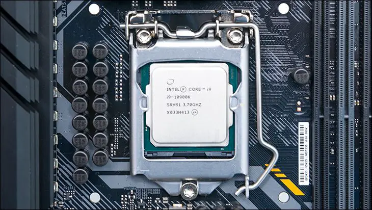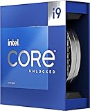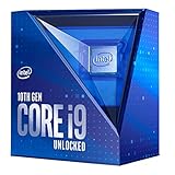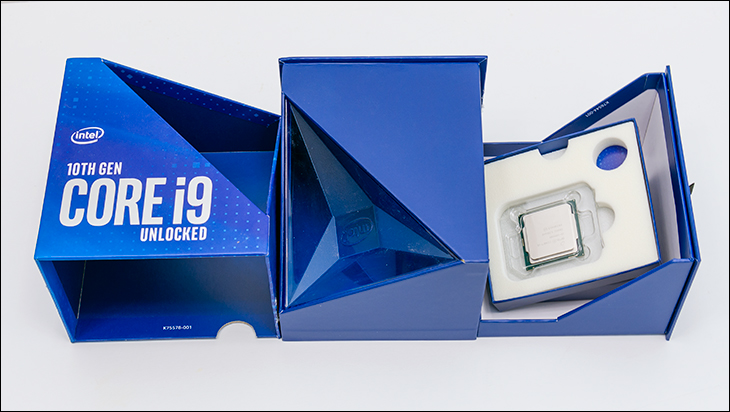
Much like previous Intel Coire i9 models, the latest and greatest 10th generation i9-10900K comes in a rather fancy box. Consisting of plastic and carboard it certainly does make a good first impression. While we doubt (m)any buyers make an impulse buy on their CPU you certainly will not confuse this new i9 with its smaller i7 and i5 brethren. Mix in the nice ‘drawer’ configuration and this is a shipping container that can take a beating without letting any of the damage actually reach its precious cargo. Honestly, we doubt many would guess that this is a sub-550 dollar processor and not a 1K+ processor, as Intel has pulled out all the stops to make it look and feel like a premium home user product.
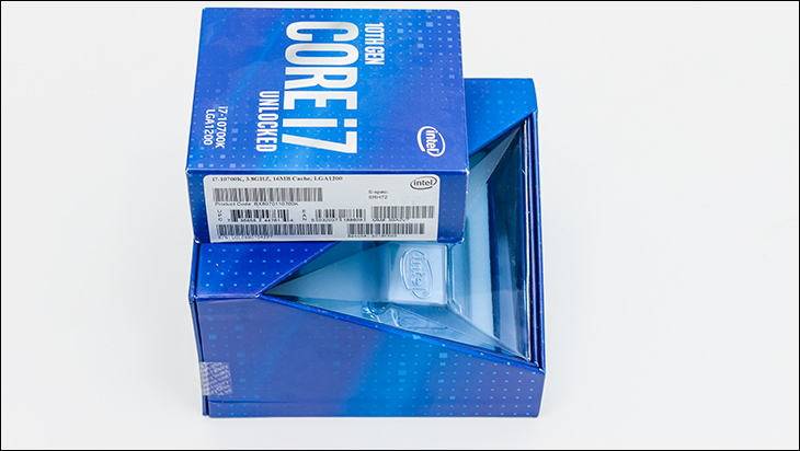
The only downside is it is a much, much bigger box. Big enough we doubt you will be able to tuck it into your motherboard’s empty container and stick it all in a safe place.

Let’s start with the angry elephant in the room. The Core i9 10900K is a 14nm(+++) based processor. Intel gets a lot of flak over this ‘recycling’ and sadly a lot of people use it to bash Intel over. So much so it has become a pet peeve of ours. When we were young, and had to walk up hill both ways to get to college, a process node’s size rating was typically related to the length of the gate / M1 half pitch. It worked as a quick and dirty way of comparing companies’ tech as engineers were in charge of the standards (i.e. complicated but somewhat grounded in reality). Even then it was of limited use beyond getting a ballpark idea of how fast you could push it, and how hot it would run. With the move to 3D structures (e.g. FinFet)… marketing has taken this standard and made it a ‘standard’ that no longer really corelates to much.

(image courtesy of der8auer’s youtube video https://youtu.be/1kQUXpZpLXI?t=797)
Put bluntly looking at the node process size is not good, beyond being fanboi fodder, for anything beyond judging company A’s last gen vs company A’s latest gen. You cannot directly compare Intel vs TSMC vs Samsung vs etc. etc. etc. It is like comparing a chess game to checkers and thinking the third guy playing poker is winning. For example Intel’s 14nm uses a fin pitch of 42nm, minimum metal pitch(MMP) of 52nm, and Contacted Gate Pitch(CPP) of 70nm. TSMC’s “7nm” uses a fin pitch of 30nm, with a CPP of 64nm, and MMP of 40nm. So TSMC’s “7nm” is smaller and newer tech, but it is not “oh my god that is a massive difference111!!!111!!!1!!!!!!”
Simply put. Intel 14nm+++ is indeed an older node process tech with lower density (37.5 Mega-Transistor per squared millimeter vs TSMC 7nm’s 96.49MTr/mm2) but shear density is not the be all and end all. Instead, it just costs more wafer space to produce the same transistor count processor than it would on a smaller process node. Equally important… There Is No Such Thing As A Free Lunch. Smaller transistor size means more issues that range from the exotic like higher likely hood of quantum tunneling, to the mundane like heat dissipation. Those issues take time and money to solve. So it not like this material and time savings per CPU is passed on to the buyer. Should Intel not retire their 14nm process and continue using it? Oh hell no. They are in the middle of the “core wars” which at some point (while no one was paying attention) replaced the MHz wars… and is about as equally important given how few home users will stress 8 or even 6 cores often enough to consider it ‘limiting’. Without a smaller node process, we are not going to see Intel match AMD in core count anytime soon. IE socket 1200’s limit is 10 cores + iGPU, a number AMD surpassed a while ago. So yeah, Intel needs to get off the stick and get their ‘10nm’ process out the door… but it is not as cut and dry as comparing node process size would lead one to believe.

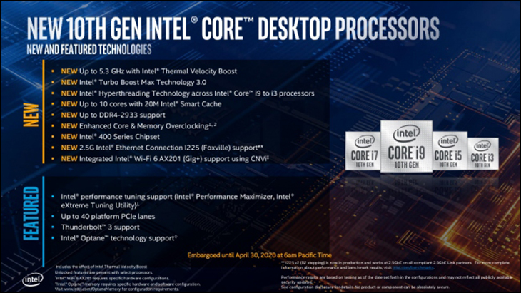
On the positive side, by using such a mature tech (Intel’s 14nm node process debuted in Core i 5th gen processors) Intel has a loooot of time to refine their design. So much so breaking the 5GHz barrier is not only possible but routine. The 10900K comes with a single core boost clock of upward of 5.3Ghz (5.2 if the CPU is above 70c and Thermal Velocity Boost cannot kick in), and can easily be overclocked to make all its cores not only hit above 5Ghz but hitting anywhere from 5.1 to 5.3Ghz very possible. That is a loooot of number crunching when dealing with twenty simultaneous threads worth of power.
This brings us to that caveat on the various core boost numbers that Intel now includes. Back in the day you had the speed a given processor was rated for and we liked it. You bought a 33Mhz processor and you got a 33Mhz processor. Nothing more, nothing less. At some point engineers realized that with multi-core processors not all the cores are stressed all the time. In order to take advantage of its TDP rating they allowed a core to go higher than the others cores. Intel called it Turbo Boost and it was good. Then with more and more cores becoming the norm those engineers realized that there are times when more than one core is active but most still are idle… so they created more “gears” in between the single core boost and base clock. In the case of Intel, they refined this ‘boost’ and dubbed it Turbo Boost 2.0. With this tech you get a higher single core and dual core boost frequency… but also a higher ‘multi core’ frequencies.

Depending on power draw (as it has to respect its TDP rating… kinda sorta), temperatures and how many cores are active this can vary greatly, but generally speaking the rated ‘base’ frequency only happens with really bad cooling and all cores are being used. Then came along Turbo Boost 3.0 which not only boost higher than TB2, it knows which cores are ‘better’ than the others and favors them when it needs to boost frequencies of a few cores(aka ‘favored cores’). Up until now this was a High End Desktop (HEDT) and Server CPU only feature. Now consumers of i7 and i9 CPUs get TB3.0. So, in practical terms, with the Corie i9 10900K what all this means is that the all-core boost is now 4.9Ghz, five core (aka half the cores active) boost is 5.0Ghz, three core boost is 5.1Ghz, and dual or single core boost is 5.2Ghz. Yes, it is confusing. It however maximizes performance while keeping temperatures and power usage at optimum levels. All automagically and without any end-user intervention needed.
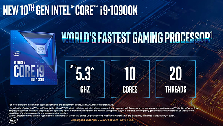
With their late 8th mobile and 9th generation desktop, Intel added another layer to its boost algorithms. Dubbed “Thermal Velocity Boost” (TVB). With this latest generation, TVB tacks on an additional 100Mhz to the single core and all core boost frequencies. However, there are few caveats. Technically it is only supposed to kick in when CPU temperatures are 70 degrees Celsius or lower, and only for short periods of time with a… ‘Tau’ or 56 second time limit. So cooling is paramount… ish. In reality TVB’s real world performance depends just as much on the motherboard used as it does cooling. Many motherboard manufactures are ignoring Intel’s TVB specifications and letting things go higher and longer than ‘it is supposed to’… but generally speaking you can expect to see frequencies bounce between 5.1Ghz and 5.3Ghz on any decent motherboard running a 10900K processor.
The reason Intel is not coming down on them like the hammer of god is because in addition to all this Intel also introduced a few other features related to power consumption. In addition to the typical 125watt TDP, or “Power Level 1” (PL1) rating as it is now called, certain 10th gen CPUs come with an even higher PL2 rating than the 9th generation. A Power Level 2 rating relaxes the power draw limit and allows the motherboard and CPU to push things harder. With the 9th gen i9-9900K, the PL2 was set to 118watts (or a mere 25 percent’ish over its 95 watt TDP) and was allowed to stay at PL2 settings for up to 28 seconds. With the tenth generation… Intel has taken a much more relaxed approach. Firstly, PL2 doubles the TDP (in the 10900K that means 250 watts) for 56 seconds and does not have to be fully respected by the motherboard manufactures. Basically, Intel now allow motherboard manufactures to consider the time limitation (aka ‘Tau’) to be a suggestion and not a hard and fast limit. Yes, Intel is now trusting the motherboard manufactures to tailor a given motherboard’s sustained power draw limits as they see fit… as they are the ones designing the VRM. Better VRM equipped boards will let TBV boost longer and higher than Intel ever dreamed of. That is a complete 180 from Intel’s rather stringent enforcement of their specifications from past years… and is what competition brings to consumers.
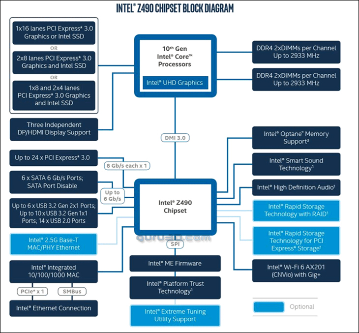
Not much has changed on the iGPU front – as it still is an Intel UHD Graphics 630, but it is more than what Ryzen big core count models come with. More importantly, if you are not using the iGPU that 15 watts of TDP goodness can be moved over to the CPU cores (and why PL2 is 250watts and not 235). The same is true of the number of PCIe lanes. Intel is sticking with 16 lanes via the CPU and the Z490 chipset supplying an additional 24 lanes. This is a bit less than what Ryzen offers at 16 with an addition 4 for NVMe and 4 more for odds ‘n’ sods. Thus, those who run fast NVMe drives will notice the slight increase in latency from the data packets going through the chipset before reaching the CPU. Though most storage enthusiasts will notice the lack of PCIe 4.0 long before they notice a difference in latency… even if the Intel socketed motherboard comes with PCIe 4.0 abilities as that is ‘future proofing’ for when gen 11 lands and is just a CPU swap. Once again, Intel 10th gen is PCIe 3.0 only, whereas AMD has been using PCIe 4.0 for awhile now.
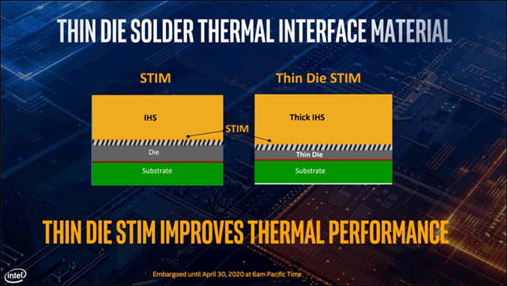
The same is true of the actual layout and architecture of the 10th generation. It still is a ‘monolithic’ core design that relies on a ring bus. Arguably, while Intel were refining things, they did find room for an additional two cores in the design but one could argue that it is the ‘same’ as the previous i9 9900K. Of course, those who do make such an argument would be wrong. Intel did not just add in two more cores and call it a day. They did not just figure out how to refine the process and boost performance and call it day. They also made the actual die height lower. Modern CPUs are flip chips with the ‘bottom’ silicon substrate layer being ‘on top’ and the transistors below them. A lower z-height in this substrate means that the heat from the cores has less bulk to travel through before it reaches the IHS. In order to keep the overall height the same, Intel then made the copper Integrated Heat Spreader thicker. When you mix in the carried over soldered TIM to the equation, temperatures across all the cores are going to be more stable than its predecessors… when good (preferrable water based) cooling solutions are used. No refinement will make a piddly little air cooler handle 250 watts of heat generation. This is why Intel once again does not bother to include a ‘stock’ cooling solution. For most people this change will not matter much, but for overclocking it is always the hottest core that is the limiting factor on ‘all core’ overclocks. Thus, having the hottest and coolest be closer in temperatures is a Good Thing™.

Also on the positive side, Hyper-Threading adjustments have been improved. Yes, not all of 10th generation CPUs get HT but those that do now can have the HT enabled or disabled on a per core basis. Not the all or nothing of previous generations. Depending on workloads this can indeed help make a heavy overclock stable… and is just plain fun to play with. Also firmly in the fun category, is the DMI chipset bus can now be easily overclocked, as the PCIe clock domains are now decoupled. What this means is you can really dial in an old school overclock and not have to worry about PCIe overclock crashing your video card and the entire system. Instead, you just have to be careful what you stick in the topmost PCIe 16 slot as its clock rate is still coupled to the DMI but the rest are not. I.E. They will run at 100Mhz while the DMI is running at whatever you find is stable for your CPU and your system. Nifty.
Falling somewhere in between these two is the upgraded onboard “Smart Cache”. On the one hand there is now 20MB of L3 and more L1 and L2 in total… on the other it is the same amount per core as the 9th generation. It is just larger because there are ten cores instead of eight. So while more gets cached it is only a continuation of the evolution of the Intel Core monolithic design.
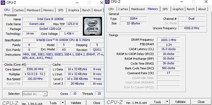
As is our want, we did push this i9 fairly hard and it is a lot of fun to play with. This is an area Intel excels at and has for many years. With ten cores of power we seriously doubt the typical buyer will be less than impressed with what can be done. Depending on what you are interested in you should easily be able to either hit 5.4-5.5Ghz on single core overclock, or 5.2-5.3 on all ten cores. It really will come down to silicon lotter, and cooling… as this fairly mild-mannered processor turns into a raging beast that eats power and spits out heat like there almost is no tomorrow when overclocked. Expect it to consume 250+ watts and need a CPU cooling solution rated for 250watt TDP or greater if you do not want it to thermally limit. For example, with a 360mm AIO cooling solution we saw temperatures in the 90s. As such it is a lot of fun, but you have to be able to handle that level of heat output before you do overclock it. The simplest recommendation is to treat it like an older HEDT, and respect what it can demand or you are going to have a less than fun time.
Either way, we personally think it is worth the effort as there is something almost giggly worthy about having 20 threads churning along at 5.3Ghz. Better still, you do not need to be a hardcore overclocking enthusiast with decades of experience to get the most from your new i9. Motherboard manufacturers have had many, many years to refine their BIOS and it does show. So much so that many will not even need to enter the BIOS and instead their motherboard will come with software that will do all the heavy lifting for you. Even Intel and their Extreme Tuning Utility (XTU) turns what was once an esoteric art into a routine task.
We personally prefer BIOS based options, but once again that is not any great hardship. If you want to pretend to be a bit of 1337 over-clocker you can do it fully manual, but most will either use the BIOS auto-tune options or at the very least some of the overclocking pre-sets. For example,ASUS typically includes a couple decent TPU overclocking gears but honestly with this tenth gen all you need do is turn on (what Asus calls) Multi-Core Enhancement, dial in the vcore and various voltages and let her rip. Depending on your motherboard you will also have to watch for vdroop but once again a couple moments in your BIOS to make the VRM more aggressive in voltage handling will also take care of that. Since we are dealing with a loaner we did not want to push so much voltage that we killed it. Instead, we made sure it did not ever go above 1.45v (which is high but not ‘its Dead Right There’ / ‘suicide run’ high).
The same is true of RAM overclocking. This latest and greatest 10th gen comes with DDR4-2933 support baked right in, and overclocking RAM is so easy that it is almost criminal to not do it. Turning our Crucial DDR4-3200 into DDR4-3600 took mere moments, and went just as high as we were able to get on this kit of RAM when using Ryzen 3000-series processors. All told, for both RAM and CPU overclocking, you are looking at a few moments worth of work at the most and a few mouse clicks at the least. In return you get a processor that out and out destroys even the most demanding tasks.
This combination means that we truly doubt the vast majority of buyers will ever feel limited by ‘only’ having ten cores. Honestly, if it had quad memory controller and more PCIe lanes we would switch back to it from HEDT end of the pool in a heartbeat. Less expensive no longer means less impressive.
